LED patterned substrate with main patterns and secondary patterns and LED chip
A technology for patterning substrates and main patterns, applied in electrical components, circuits, semiconductor devices, etc., to achieve the effect of improving the light extraction rate of LEDs
- Summary
- Abstract
- Description
- Claims
- Application Information
AI Technical Summary
Problems solved by technology
Method used
Image


Examples
Embodiment 1
[0026] 1 is a schematic diagram of the LED chip of this embodiment, which consists of an LED patterned substrate 11 with primary and secondary double patterns, an N-type GaN layer 12, an MQW quantum well layer 13, and a P-type GaN layer 14 arranged in sequence.
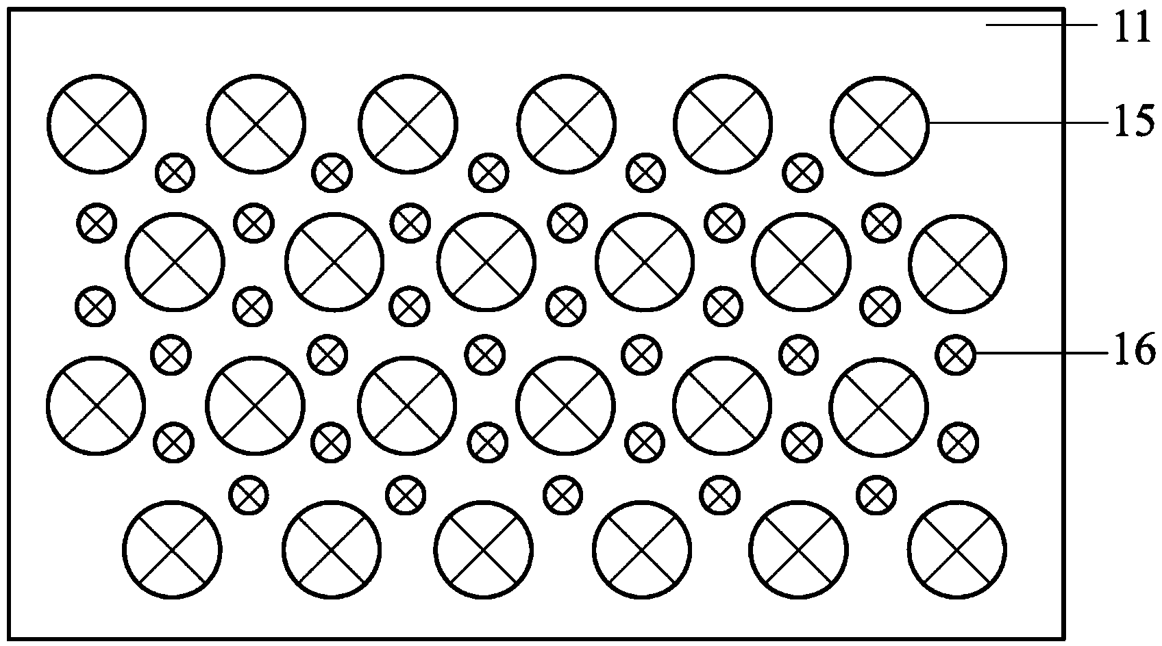
[0027] Such as figure 2 As shown, in the LED patterned substrate with primary and secondary double patterns in this embodiment, the pattern on the substrate is composed of the main pattern 15 and the secondary pattern 16 arranged on the surface of the substrate; the main pattern and the secondary pattern are of the same type Pattern, that is, the cone pattern; where, such as Figure 2~3 As shown, the base circle radius r of the main pattern cone 1 1.5μm, inclination α 1 60°, the distance between the centers of adjacent main patterns is 5.0 μm, and the arrangement is hexagonal; the radius of the bottom circle of the sub-pattern cone is 0.7 μm, the inclination angle is 45°, and it is arranged in the gap of the main pa...
Embodiment 2
[0041] The LED chip of this embodiment is composed of an LED patterned substrate with primary and secondary double patterns, an N-type GaN layer, an MQW quantum well layer, and a P-type GaN layer arranged in sequence.
[0042] Such as Figure 4 As shown, in the LED patterned substrate with primary and secondary double patterns in this embodiment, the pattern on the substrate is composed of the main pattern 25 and the secondary pattern 26 arranged on the surface of the substrate; the main pattern 25 and the secondary pattern 26 are used for the main pattern Different patterns. Such as Figure 4~5As shown, the main pattern adopts a regular hexagonal pyramid pattern, and the inclination angle α of the regular hexagonal pyramid pattern 2 is 60°, side length a 2 is 1.0 μm, the distance between the centers of adjacent regular hexagonal pyramids is 3.2 μm, and the arrangement is hexagonal; for example Figure 4 , 6 As shown, the secondary pattern is a hemisphere, and the radius ...
Embodiment 3
[0056] The LED chip of this embodiment is composed of an LED patterned substrate with primary and secondary double patterns, an N-type GaN layer, an MQW quantum well layer, and a P-type GaN layer arranged in sequence.
[0057] Such as Figure 7 As shown, in the LED patterned substrate with primary and secondary double patterns in this embodiment, the pattern on the substrate is composed of a main pattern 35 and a secondary pattern 36 arranged on the surface of the substrate; the main pattern 35 and the secondary pattern 36 are used for the main pattern Different patterns. Such as Figure 7-8 As shown, the inclination angle α of the regular triangular pyramid used in the main pattern 3 is 45°, the side length of the regular triangular pyramid is a 3 is 2.0 μm, the distance between adjacent main patterns is 5.0 μm, and the arrangement is rectangular; for example Figure 7 , 9 As shown, the secondary pattern adopts a regular hexagonal pyramid, and the inclination angle α 4 ...
PUM
 Abstract
Description
Claims
Application Information
 - R&D
- Intellectual Property
- Life Sciences
- Materials
- Tech Scout
- Unparalleled Data Quality
- Higher Quality Content
- 60% Fewer Hallucinations
Browse by: Latest US Patents, China's latest patents, Technical Efficacy Thesaurus, Application Domain, Technology Topic, Popular Technical Reports.
© 2025 PatSnap. All rights reserved.Legal|Privacy policy|Modern Slavery Act Transparency Statement|Sitemap|About US| Contact US: help@patsnap.com