Laser imaging processing device

A processing device and laser imaging technology, which is applied in the direction of photolithography exposure device, microlithography exposure equipment, etc., can solve the problems of reduced productivity and product quality, film expansion and shrinkage, and cumbersome procedures, etc.

Inactive Publication Date: 2014-01-29
SUZHOU DELPHI LASER
View PDF4 Cites 0 Cited by
  • Summary
  • Abstract
  • Description
  • Claims
  • Application Information

AI Technical Summary

Problems solved by technology

[0003] The traditional printed circuit exposure method is to use ultraviolet light to irradiate the photomask, which requires the addition of a photomask film during the processing process. In this method, because the uniformity of ultraviolet light is not the same, the repeatability of the line width near the edge is not good; In addition, there is a problem of expansion and contraction of the film, which will affect the accuracy. There will be an error of tens to hundreds of microns on the 500mm circuit board; with the development of circuit board technology, the required size of the circuit board circuit becomes more and more Fine, resulting in a reduction in productivity and product quality, at the same time, the traditional single laser head processing to reach the exposure pattern cycle is longer, the process is more cumbersome

Method used


Image

  • Laser imaging processing device
  • Laser imaging processing device

Examples


Embodiment Construction

[0020] The present invention will be described in detail below in conjunction with specific embodiments shown in the accompanying drawings. However, these embodiments do not limit the present invention, and any structural, method, or functional changes made by those skilled in the art according to these embodiments are included in the protection scope of the present invention.

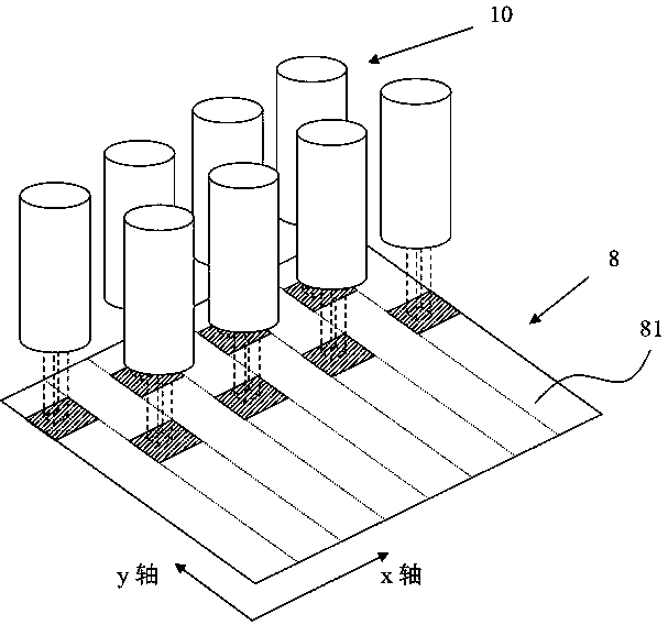
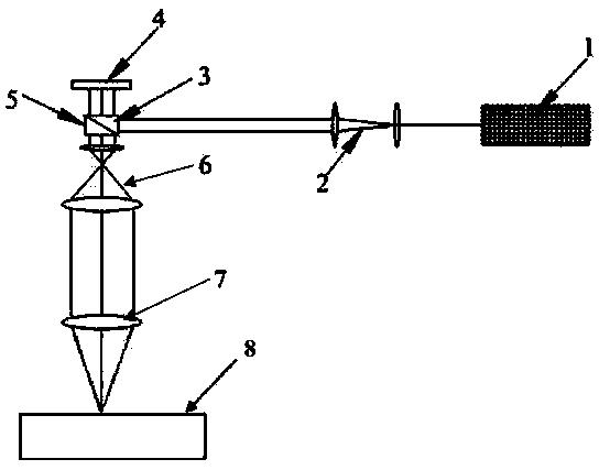
[0021] Please refer to figure 1 Shown is a laser imaging processing device according to an embodiment of the present invention, which includes: a working platform 8 and several exposure devices 10 facing the working platform 8 . In particular, the exposure devices 10 adjacent to each other in the X-axis direction of the work platform 8 are provided with a distance in the Y-axis direction of the work platform 8, and the exposure devices 10 project a number of light spots on the work platform 8. The projections on the X-axis line up. Of course, in other embodiments, the pattern formed by the light spot...


PUM


Abstract

The invention discloses a laser imaging processing device. The laser imaging processing device comprises a plurality of exposure devices and a working platform, wherein the exposure devices adjacent in the X axis direction of the working platform are arranged at intervals in the Y axis direction of the working platform; a plurality of light spots are projected on the working platform by the exposure devices, and the projections of the light spots on the X axis are connected into a line. The laser imaging processing device utilizes a plurality of exposure devices to carry out exposure work at the same time, controls the parameters of the light spots, such as shapes, sizes and grey levels through the angle of each exposure device, and carries out quick exposure treatment on a circuit board by combining the movable working platform to solve the problem of inaccurate processing caused by no expansion of negative plates in the exposure face, and meanwhile, a focused laser beam can process extremely precision circuits.

Description

technical field [0001] The invention relates to the technical field of laser processing equipment, in particular to a laser imaging processing device. Background technique [0002] Maskless lithography technology, also known as direct imaging, has excellent advantages in products such as semiconductors and personal computer motherboards. Video technology not only saves costs, but also makes it more flexible in use. The main working mode is to directly use the data output by the CAM workstation to drive the laser imaging device to perform graphic imaging on the printed circuit board coated with photoresist. [0003] The traditional printed circuit exposure method is to use ultraviolet light to irradiate the photomask, which requires the addition of a photomask film during the processing process. In this method, because the uniformity of ultraviolet light is not the same, the repeatability of the line width near the edge is not good; In addition, there is a problem of expans...

Claims


Application Information

Patent Timeline
Patent Type & Authority Applications(China)
IPC IPC(8): G03F7/20
Inventor 赵裕兴狄建科姜尧张伟李金泽蔡仲云
Owner SUZHOU DELPHI LASER
Why Eureka
Try Eureka