Device and method for processing laser direct imaging

A technology of laser direct imaging and processing equipment, applied in laser welding equipment, metal processing equipment, welding equipment, etc., can solve the problems of reduced productivity and product quality, poor line width repeatability, and impact on precision, and achieve processing efficiency High, simple operation, high-precision effect

Active Publication Date: 2013-04-10
SUZHOU DELPHI LASER
View PDF8 Cites 4 Cited by
  • Summary
  • Abstract
  • Description
  • Claims
  • Application Information

AI Technical Summary

Problems solved by technology

[0003] The traditional printed circuit exposure method is to use ultraviolet light to irradiate the photomask, which requires the addition of photomask film during the processing process. In this method, because the uniformity of ultraviolet light is not the same, the repeatability of the line width near the edge is not good; In addition, there is a problem of expansion and contraction of the film, which will affect the accuracy. There will be an error of tens to hundreds of microns on the 500mm circuit board; at the same time, with the development of circuit board technology, the required size of the circuit board circuit becomes more and more The thinner it is, the lower the productivity and product quality

Method used


Image

  • Device and method for processing laser direct imaging

Examples


Embodiment Construction

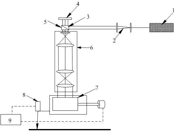
[0016] Such as figure 1 As shown, the laser direct imaging processing device is arranged with a first beam expander 2 at the output end of the ultrashort pulse laser 1, and the output end of the first beam expander 2 is provided with a first 45-degree half mirror 3, and the first 45 The reflection output end of the half-mirror 3 is arranged with a DLP chip 4, the output end of the DLP chip 4 is arranged through the second 45-degree half-mirror 5, and the transmission output end of the second 45-degree half-mirror 5 is arranged with a second beam expander Mirror 6, the second beam expander mirror 6 is facing the working platform, the working platform includes an X-axis transmission unit, a Y-axis transmission unit and a high-temperature-resistant ceramic substrate, and the X-axis transmission unit includes an X-axis slide rail and controls the movement of the X-axis slide rail The Y-axis transmission unit includes the Y-axis slide rail and the motor that controls the movement o...


PUM


Abstract

The invention relates to a device for processing laser direct imaging and a method for processing laser direct imaging. An ultrashort pulse laser sends out laser to enter a first beam expander, beam amplification is realized through the first magnification-adjustable beam expander, the laser enters a digital light processing (DLP) chip through a first 45-degree semi-reflective mirror, the DLP chip is controlled through a computer aided manufacturing (CAM) workstation, the CAM workstation directly outputs images to the DLP chip, a digital micromirror device (DMD) system in the DLP chip modulates the beam, the modulated beam transfers a second 45-degree semi-reflective mirror, is amplified or focused through a second magnification-adjustable beam expander and is focused on a printed circuit board under the action of the second beam expander, before the processing, a charge coupled device (CCD) sensor senses a sample position and corrects the sample position together with an auto focus (AF) unit, so that light path correction is carried out. The device has the characteristics of simplicity in operation, high processing sample fineness, good quality, high working efficiency and the like.

Description

technical field [0001] The invention relates to a laser direct imaging processing device and a method thereof, belonging to the technical field of laser processing equipment. Background technique [0002] Maskless lithography technology, also known as direct imaging, has excellent advantages in products such as semiconductors and personal computer motherboards. Video technology not only saves costs, but also makes it more flexible in use. The main working mode is to directly use the data output by the CAM workstation to drive the laser imaging device to perform graphic imaging on the printed circuit board coated with photoresist. [0003] The traditional printed circuit exposure method is to use ultraviolet light to irradiate the photomask, which requires the addition of a photomask film during the processing process. In this method, because the uniformity of ultraviolet light is not the same, the repeatability of the line width near the edge is not good; In addition, ther...

Claims


Application Information

Patent Timeline
IPC IPC(8): B23K26/073B23K26/08
Inventor 赵裕兴狄建科姜尧益凯劼
Owner SUZHOU DELPHI LASER
Why Eureka
Try Eureka