FPGA-based (field programmable gate array-based) USB (universal serial bus) to multilink interface circuit

An interface circuit and road link technology, applied in the field of electronic circuits, can solve the problems of increasing circuit cost and complexity, slow JTAG transmission speed, affecting data transmission speed, etc., to achieve the effect of improving transmission speed

Active Publication Date: 2013-11-27
XIDIAN UNIV
View PDF3 Cites 4 Cited by
  • Summary
  • Abstract
  • Description
  • Claims
  • Application Information

AI Technical Summary

Problems solved by technology

Since the transmission speed of JTAG is very slow, which directly affects the transmission speed of data, it is difficult to meet the real-time requirements in the case of high speed requirements.
In addition, in the prior art, if you want to transmit data in parallel in multiple ADSPs, you need to use multiple USB interfaces of the computer to connect multiple JTAGs, and then transmit the data to multiple ADSPs through multiple JTAGs, but this requires multiple JTAG, which adds cost and complexity to the circuit
[0003] In recent ye...

Method used


Image

  • FPGA-based (field programmable gate array-based) USB (universal serial bus) to multilink interface circuit
  • FPGA-based (field programmable gate array-based) USB (universal serial bus) to multilink interface circuit
  • FPGA-based (field programmable gate array-based) USB (universal serial bus) to multilink interface circuit

Examples


Embodiment Construction

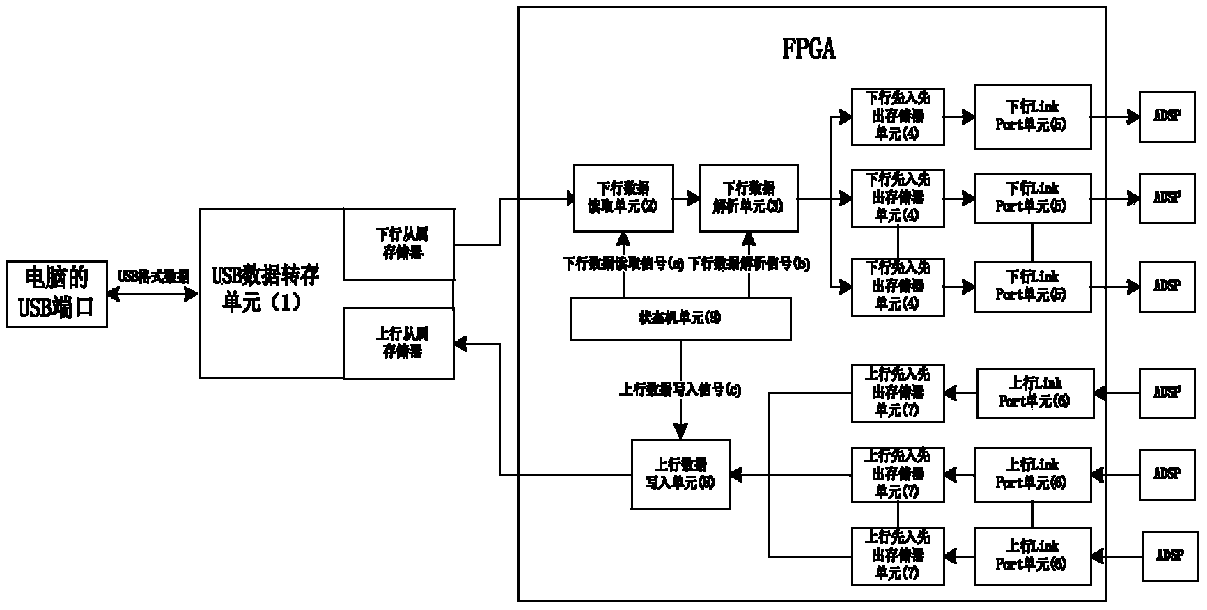
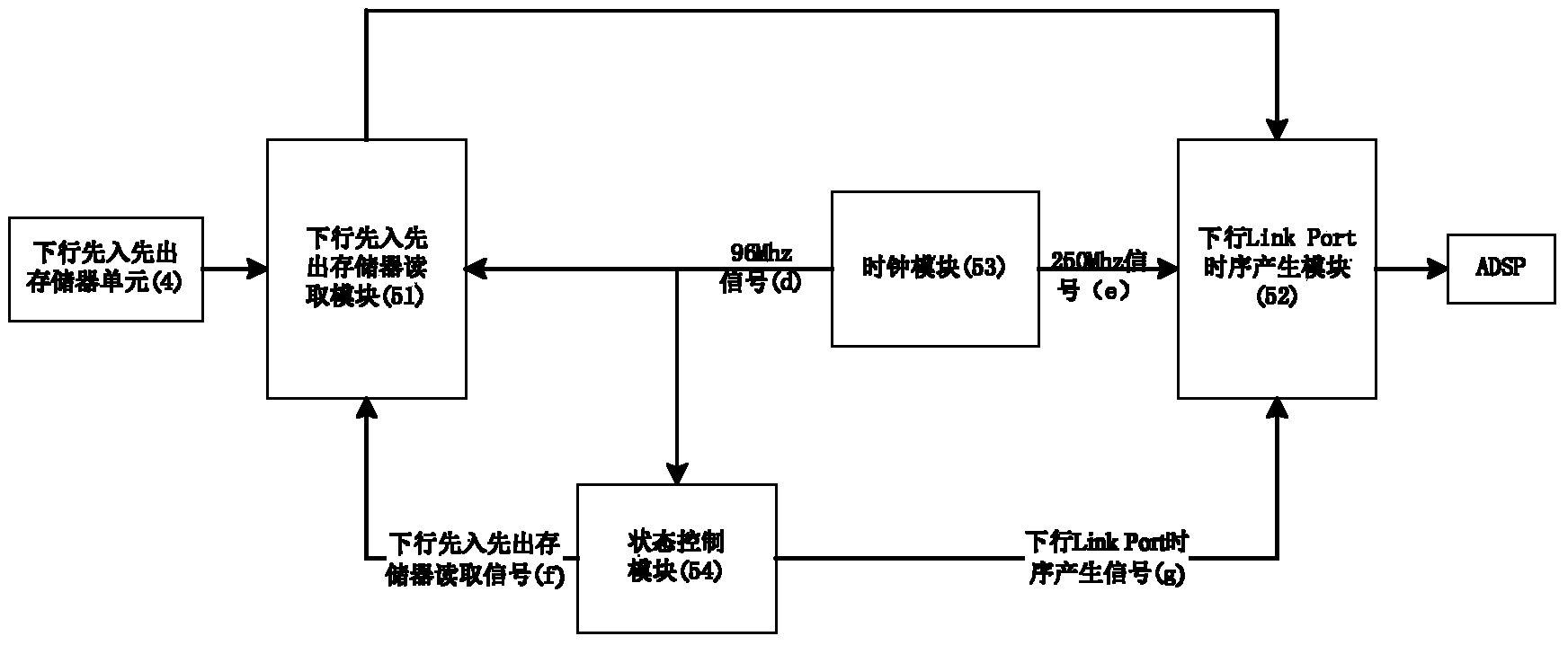
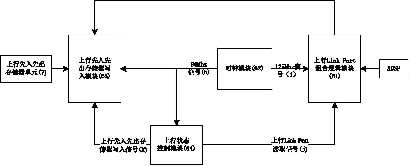
[0022] Reference figure 1 , The present invention includes: USB data transfer unit 1, downstream data reading unit 2, downstream data analysis unit 3, N downstream first-in first-out memory units 4, N downstream Link Port units 5, N upstream Link Port units 6. N upstream first-in first-out memory units 7, upstream data writing unit 8 and state machine unit 9; the USB data transfer unit 1 is composed of a CY7C68013A chip connected with a peripheral resistance-capacitance component, and the downstream data reading unit 2 , Downstream data analysis unit 3, N downstream first-in first-out memory unit 4, N downstream Link Port unit 5, N upstream Link Port unit 6, N upstream first-in first-out memory unit 7, upstream data writing unit 8 and state machine unit 9 are implemented inside FPGA, among them:

[0023] The input end of the USB data transfer unit 1 is connected to the USB interface of the computer, and the output end is connected to the downstream data reading unit 2. During dow...


PUM


Abstract

The invention discloses an FPGA-based USB to multilink interface circuit and mainly solves the problem that an existing single USB cannot be converted into a multilink interface. The FPGA-based USB to multilink interface circuit comprises a USB data transfer unit (1), a down data reading unit (2), a down data analyzing unit (3), N down FIFO (first in first out) memory units (4), N down Link Port units (5), N up Link Port units (6), N up FIFO memory units (7), an up data writing-in unit (8) and a state machine unit (9). The USB data transfer unit (1) extracts and stores USB data in the down FIFO memory units (4), and then the down Link Port units (5) send the data to an ADSP (advanced signal processing) unit; the up Link Port units (6) extract and store Link Port data in the up FIFO memory units (7), and then the USB data transfer unit (1) converts the data into USB data. The FPGA-based USB to multilink interface circuit has the advantages of simple structure and fast speed and is applicable to USB to multilink interfaces.

Description

Technical field [0001] The invention belongs to the technical field of electronic circuits, in particular to a circuit that uses FPGA to realize the conversion of a USB interface into a multi-link interface, and can be applied to parallel data transmission from a computer to multiple ADSP processors. Background technique [0002] At present, in order to transfer data from a computer to a multi-chip digital signal processor ADSP, the data is generally transmitted to one ADSP through the debugging interface JTAG, and then the data is transmitted to other ADSPs through shared memory. Because the transmission speed of JTAG is very slow, it directly affects the transmission speed of data. It is difficult to meet the real-time requirements in occasions with high speed requirements. In addition, in the prior art, if you want to transmit data to multiple ADSPs in parallel, you need to connect multiple JTAGs with multiple USB interfaces of the computer, and then transmit data to multiple ...

Claims


Application Information

Patent Timeline
IPC IPC(8): G06F13/40
Inventor 侯彪焦李成张文科白静王爽倪玉峰
Owner XIDIAN UNIV
Why Eureka
Try Eureka