A kind of array substrate and its manufacturing method and display panel

A technology of an array substrate and a manufacturing method, which is applied in the field of liquid crystal display, can solve problems such as poor display, achieve the effects of high hardness, improve user experience, and improve image display quality

Active Publication Date: 2015-08-26
BEIJING BOE OPTOELECTRONCIS TECH CO LTD
View PDF5 Cites 0 Cited by
  • Summary
  • Abstract
  • Description
  • Claims
  • Application Information

AI Technical Summary

Problems solved by technology

[0004] Embodiments of the present invention provide an array substrate, a manufacturing method thereof, and a display panel, which are used to solve the problem of bad display caused by damaged spacers in the prior art and improve the display effect of a liquid crystal display device

Method used


Image

  • A kind of array substrate and its manufacturing method and display panel
  • A kind of array substrate and its manufacturing method and display panel
  • A kind of array substrate and its manufacturing method and display panel

Examples


Embodiment Construction

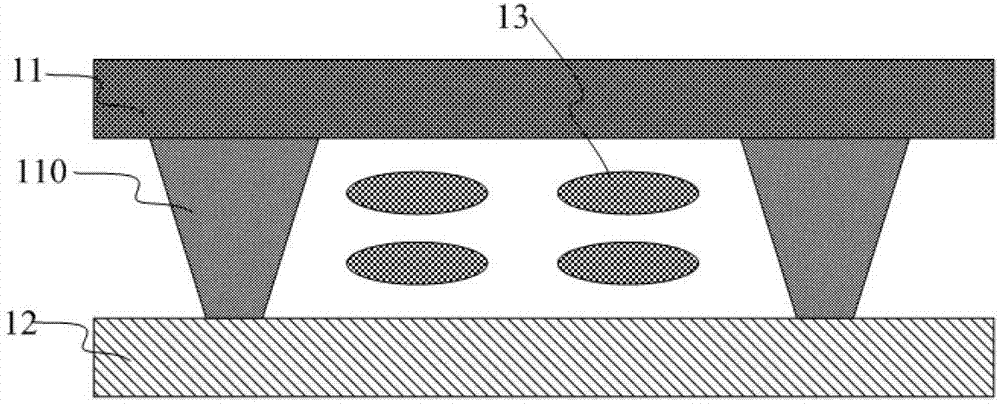
[0035] Embodiments of the present invention provide an array substrate, a manufacturing method thereof, and a display panel, which are used to solve the problem of poor display caused by damaged spacers in the prior art and improve the display effect of a liquid crystal display device.

[0036] The following will clearly and completely describe the technical solutions in the embodiments of the present invention with reference to the accompanying drawings in the embodiments of the present invention. Obviously, the described embodiments are only some of the embodiments of the present invention, not all of them. Based on the embodiments of the present invention, all other embodiments obtained by persons of ordinary skill in the art without making creative efforts belong to the protection scope of the present invention.

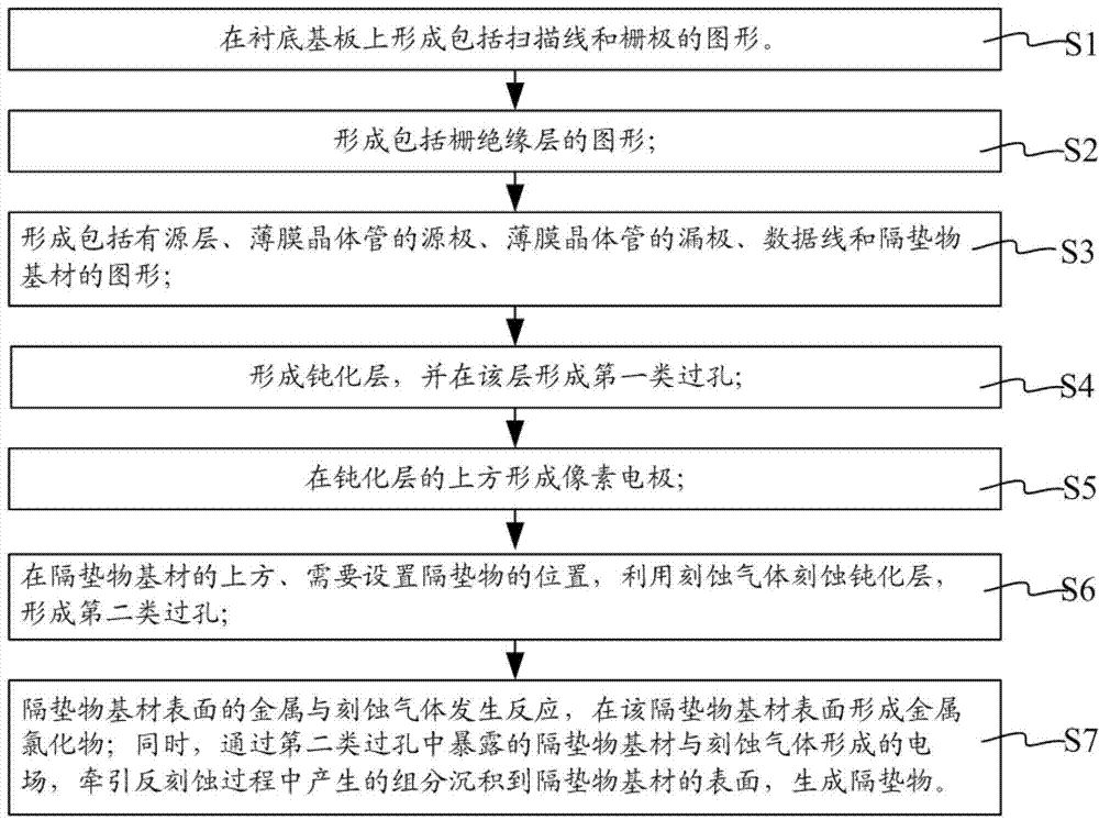
[0037] Attached below figure 2 , to introduce in detail the manufacturing method of the array substrate provided by the embodiment of the present invention, the...


PUM


Abstract

A method for manufacturing an array substrate comprises: forming a pattern comprising a scanning line and a gate (302) on a base substrate (301); forming a gate insulation layer (303) above the pattern comprising the scanning line and the gate (302); forming a pattern comprising an active layer (304), a data line (305) and a spacer base material (306) above the gate insulation layer (303); forming a passivation layer (307) above the pattern comprising the active layer (304), the data line (305) and the spacer base material (306); and etching the passivation layer (307) by using a dry etching method, so as to form a via hole (309) for exposing the spacer base material (306), and by means of an electric field formed by using the spacer base material (306) exposed in the via hole (309) and etching gas, inducing a substance generated in the etching to be deposited on a surface of the exposed spacer base material (306), so as to generate a spacer (310). Also provided are an array substrate and a display panel.

Description

technical field [0001] The invention relates to the technical field of liquid crystal display, in particular to an array substrate, a manufacturing method thereof, and a display panel. Background technique [0002] With the development of thin film transistor liquid crystal display (TFT-LCD Display) technology and the progress of industrial technology, the production cost of liquid crystal display devices has been reduced, and the manufacturing process has been improved day by day. Mainstream technology; due to its own advantages, it has become an ideal display device in the minds of the market and consumers. At present, the stereoscopic display technology is increasingly emerging in the market, so it is increasingly important to solve the technical shortcomings of the stereoscopic display technology and improve the image quality (such as reducing color shift, reducing stereoscopic crosstalk, screen flicker, increasing viewing angle, etc.). [0003] Advanced ultra-dimension...

Claims


Application Information

Patent Timeline
Patent Type & Authority Patents(China)
IPC IPC(8): G02F1/1339H01L27/12H01L21/77
CPCG02F1/13394G02F2201/503G02F1/136286G02F1/136295G02F1/133345G02F1/1368G02F1/13398
Inventor 郭建刘建涛
Owner BEIJING BOE OPTOELECTRONCIS TECH CO LTD
Why Eureka
Try Eureka