Testing jig for testing mobile phone PCB pin point conduction

A technology for testing PCB boards and mobile phones. It is applied in electronic circuit testing, parts of electrical measuring instruments, and measuring electricity. It can solve problems such as inconvenient use, crushing PCB boards, and testing equipment without lighting functions. Convenience and avoid damage effect

Inactive Publication Date: 2013-11-27
KUSN MAIZHI FIXTURE TECH
View PDF8 Cites 14 Cited by
  • Summary
  • Abstract
  • Description
  • Claims
  • Application Information

AI Technical Summary

Problems solved by technology

[0003] In order to solve the problems in the prior art that the pin-point conduction equipment of the mobile phone PCB board adopts a push-down design, which may crush the PCB board, and the testing equipment does not have a lighting function, and is not convenient to use, the present invention provides a The structure is simple, the lighting effect is good, the use is convenient, and the test fixture for testing the pin-point conduction of the mobile phone PCB board is used to test the pin-point conduction of the mobile phone PCB board by adopting a rising design to avoid crushing the PCB board.

Method used


Image

  • Testing jig for testing mobile phone PCB pin point conduction
  • Testing jig for testing mobile phone PCB pin point conduction
  • Testing jig for testing mobile phone PCB pin point conduction

Examples


Embodiment Construction

[0013] The present invention will be further described below in conjunction with the accompanying drawings.

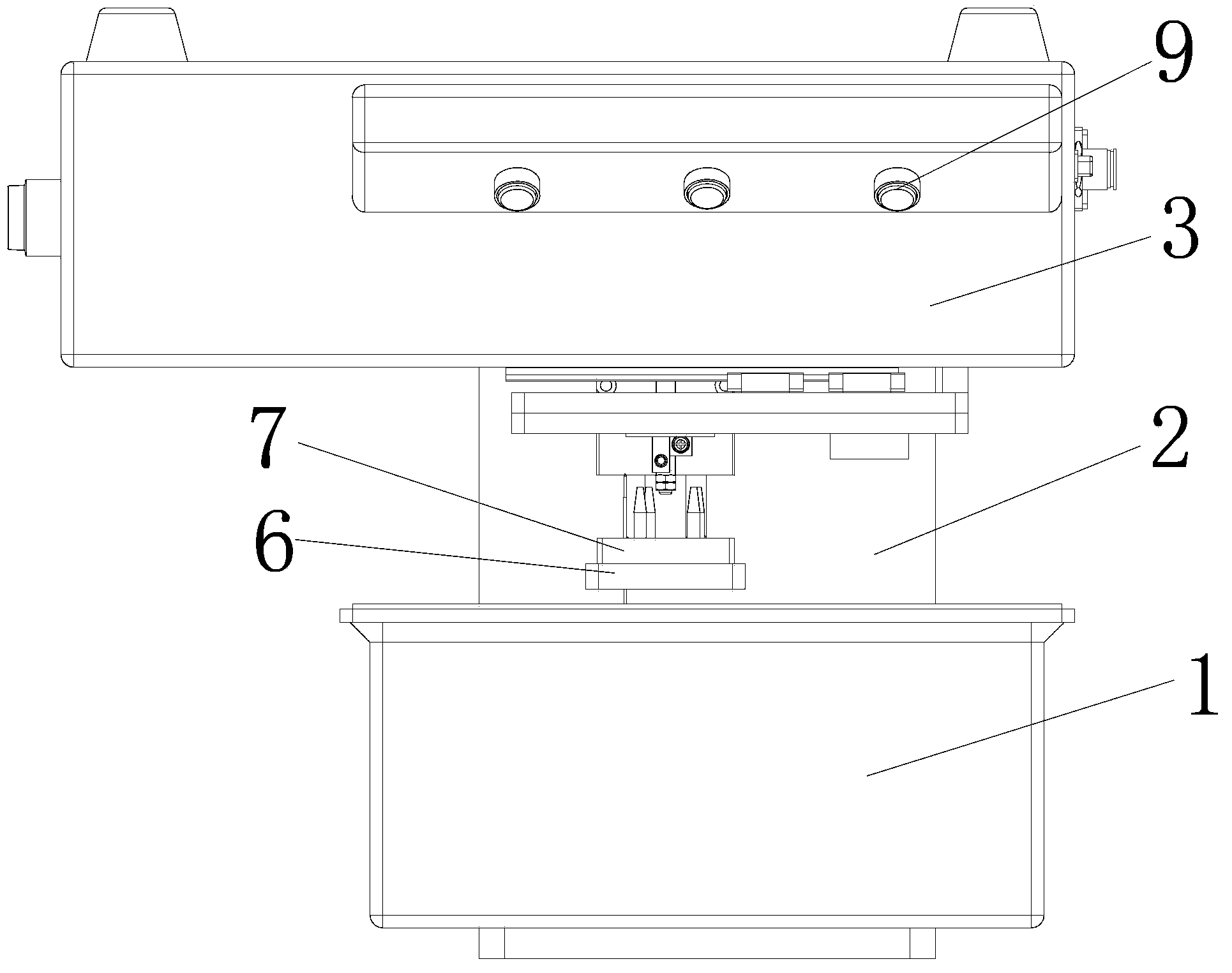
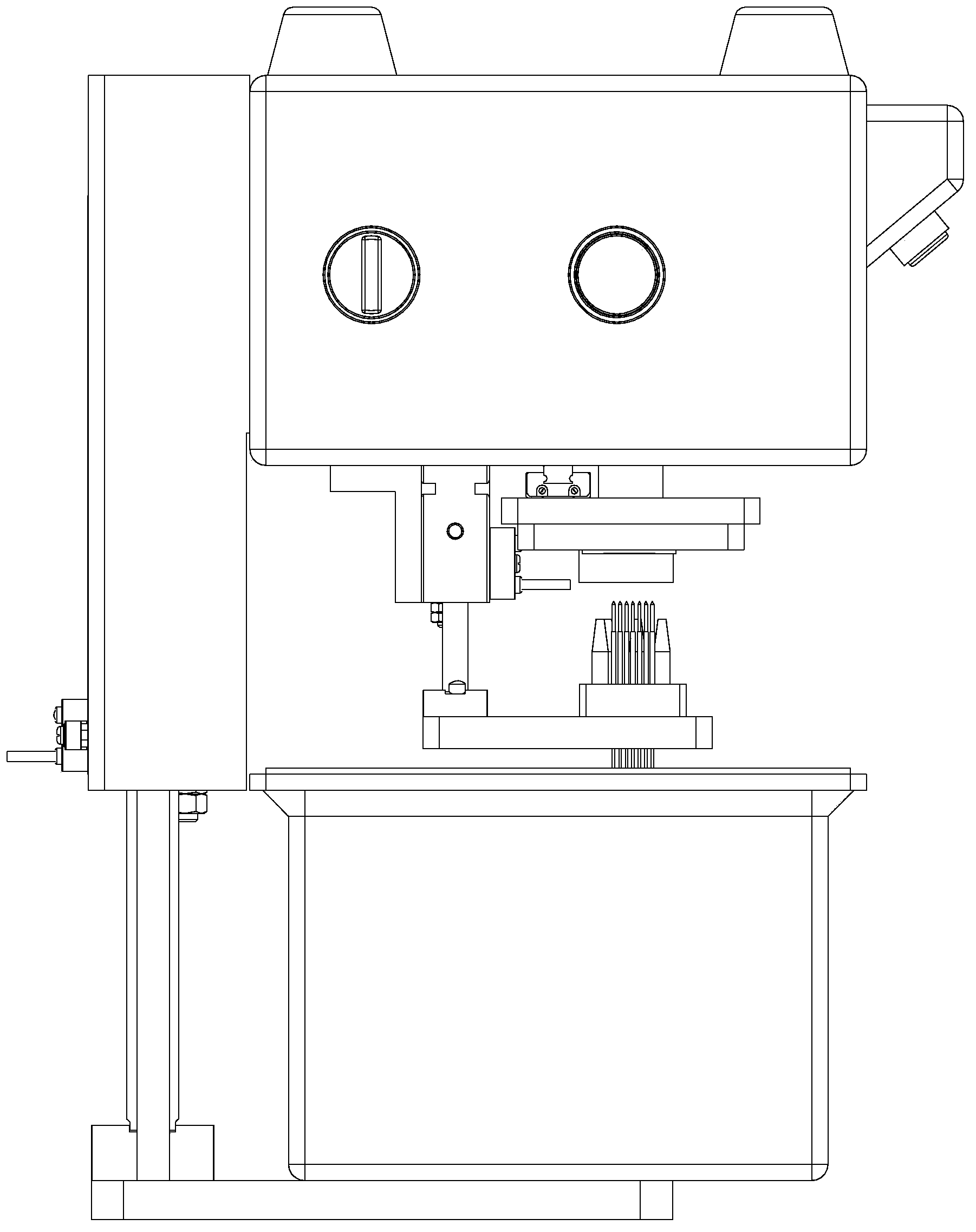
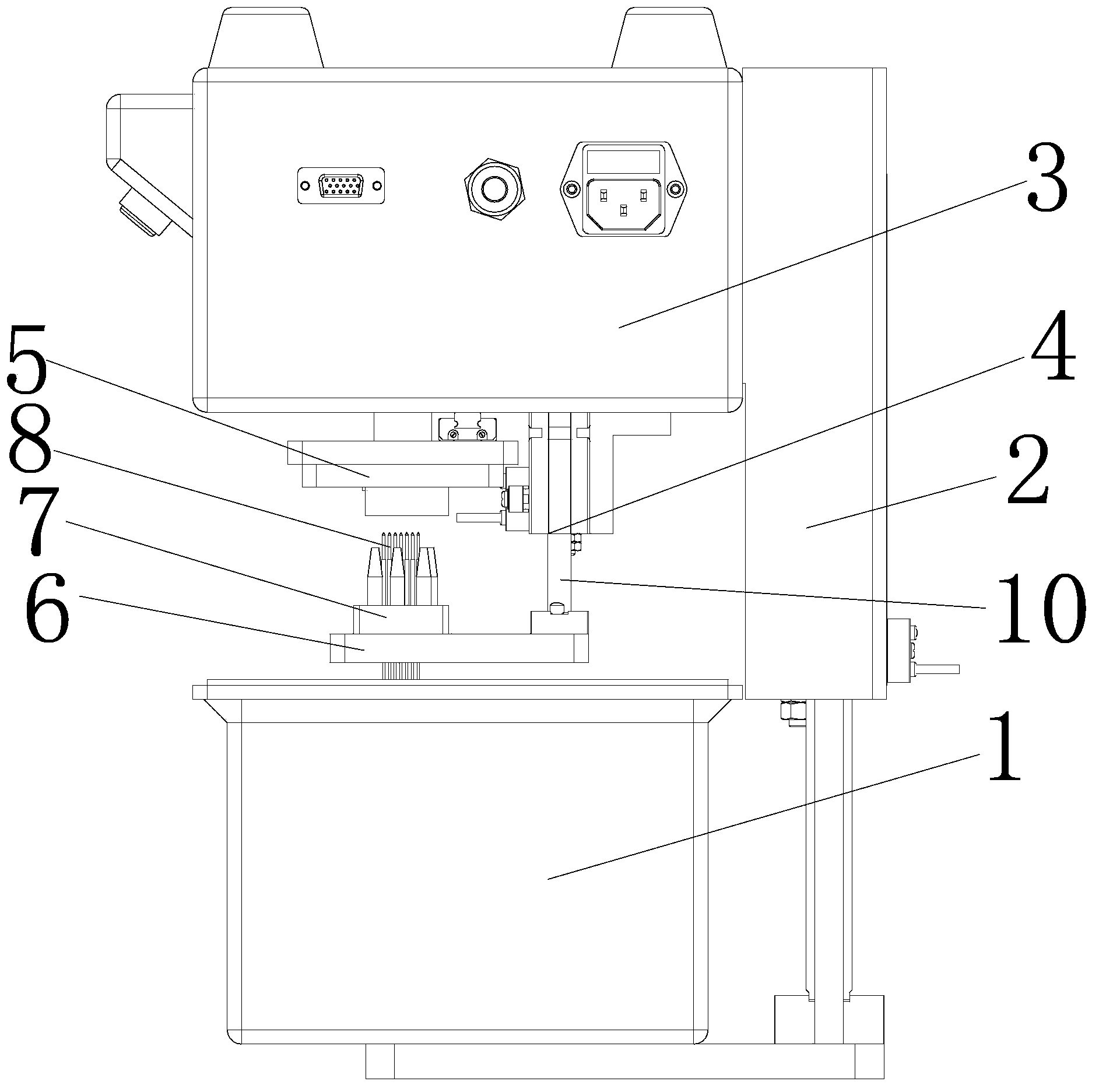
[0014] Such as Figure 1-3 As shown, a test fixture for testing the pin-point conduction of a mobile phone PCB board includes a test bench 1, a support plate 2, a top seat 3, a cylinder 4, a positioning carrier plate 5, a moving plate 6, a pin insertion plate 7 and The probe 8 is provided with a support plate 2 on the rear side of the test platform 1, and a top seat 3 located above the test platform 1 is connected to the front end of the support plate 2, and a positioning carrier plate for placing a PCB board is provided at the bottom of the front end of the top seat 3 5. A cylinder 4 is arranged at the bottom of the rear end of the top seat 3, and the cylinder rod 10 of the cylinder 4 is connected to the moving plate 6 arranged horizontally, and a pin plate 7 is arranged on the top of the moving plate 6. Set in the pin board 7 and point to the PCB board. A row of la...


PUM


Abstract

The testing jig for testing mobile phone PCB pin point conduction. The testing jig comprises a testing table and is characterized by further comprising a supporting plate, a footstock, an air cylinder, a locating carrying plate, a movable plate, a probe insertion plate and probes. The supporting plate is arranged on the rear side of the testing table. The footstock located above the testing table is connected to the front end of the supporting plate. The locating carrying plate where a PCB is placed is arranged at the bottom of the front end of the footstock. The air cylinder is arranged at the bottom of the rear end of the footstock. An air cylinder rod of the air cylinder is connected with the transversely-arranged movable plate. The probe insertion plate is arranged at the top of the movable plate. The multiple probes are arranged inside the probe insertion plate. The testing jig solves the problems that the downwards-pressing design is adopted in testing devices for testing mobile phone PCB pin point conduction, the PCB is possibly damaged due to pressing, the testing devices do not have the lighting function, and therefore use is inconvenient to achieve. The testing jig for testing mobile phone PCB pin point conduction is simple in structure, good in lighting effect and convenient to use, and the ascending design is adopted so that the PCB can be prevented from being damaged by pressing.

Description

technical field [0001] The invention relates to a test fixture, in particular to a test fixture for testing the pin-point conduction of a mobile phone PCB board. Background technique [0002] The Chinese name of board B is printed circuit board, also known as printed circuit board, which is an important electronic component, a support for electronic components, and a provider of electrical connections for electronic components. Because it is made using electronic printing, it is called a "printed" circuit board. PCB boards are widely used in a series of electronic products such as computer motherboards, mobile phone motherboards, and PAD motherboards. The PCB board of the mobile phone needs to test whether its pin points are conductive. At present, the test equipment adopts the push-down design, and the driving mechanism is used to drive the probe to press down the test. Due to the gravity of the probe, the PCB board may be crushed, causing serious damage to the enterprise....

Claims


Application Information

Patent Timeline
Patent Type & Authority Applications(China)
IPC IPC(8): G01R1/073G01R31/28
Inventor 陈国栋
Owner KUSN MAIZHI FIXTURE TECH
Why Eureka
Try Eureka