Backboard used for packaging of crystalline silicon photovoltaic module

A photovoltaic module packaging and crystalline silicon technology, which is applied in photovoltaic power generation, semiconductor devices, electrical components, etc., can solve the problems of high cost of new photovoltaic module backplane materials and manufacturing costs, and achieve flexible manufacturing methods, cost reduction, and cost reduction Effect

Inactive Publication Date: 2013-10-30
SUZHOU HAORUI NEW ENERGY TECH
View PDF0 Cites 1 Cited by
  • Summary
  • Abstract
  • Description
  • Claims
  • Application Information

AI Technical Summary

Problems solved by technology

[0006] In view of the deficiencies in the existing technology, in order to solve the problem of high material cost and manufacturing cost of the new photovoltaic module backplane, the present invention provides a new technical solution, a crystalline silicon photovoltaic module backplane

Method used


Image

  • Backboard used for packaging of crystalline silicon photovoltaic module
  • Backboard used for packaging of crystalline silicon photovoltaic module

Examples


Embodiment Construction

[0021] The present invention will be described in further detail below in conjunction with the accompanying drawings.

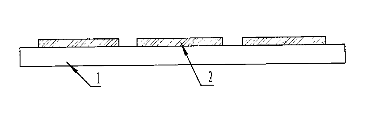
[0022] like figure 1 As shown, a backplane for crystalline silicon photovoltaic module packaging includes a backplane substrate layer 1 and a connection circuit layer 2, wherein the connection circuit layer 2 is a conductive circuit composed of metal aluminum, and the present invention replaces metal copper with metal aluminum form a conductive circuit.

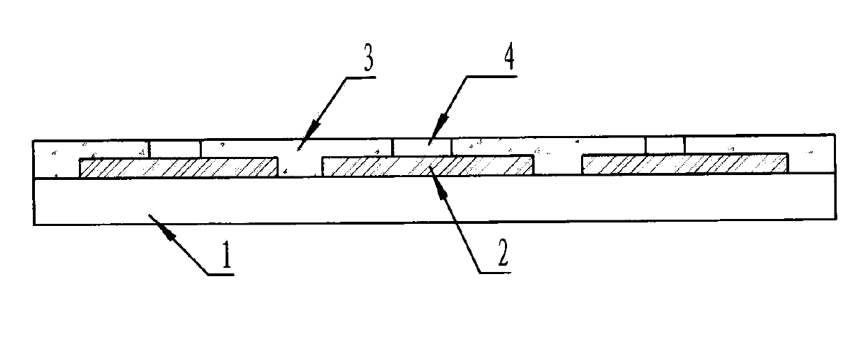
[0023] like figure 2 As shown, a backplane for crystalline silicon photovoltaic module packaging includes a backplane substrate layer 1 and a connection circuit layer 2, wherein the connection circuit layer 2 is a conductive circuit composed of metal aluminum, and the connection circuit layer 2 An insulating layer 3 is provided on the outer surface, and an electrical connection point window 4 is provided on the insulating layer 3 .

[0024] In the present invention, the backplane substrate layer 1 is com...


PUM


Abstract

The invention discloses a backboard used for packaging of a crystalline silicon photovoltaic module. The backboard used for packaging of the crystalline silicon photovoltaic module is used for leading out an electrode crystalline silicon photovoltaic cell from the packaging backboard. The backboard used for packaging of the crystalline silicon photovoltaic module comprises a backboard substrate layer and a connecting circuit layer composed of metallic aluminum instead of metallic copper. According to the backboard used for packaging of the crystalline silicon photovoltaic module, in order to improve the performance of the backboard, an insulation layer can be arranged on the outer layer of the connecting circuit layer, and electrically connected point windows are formed in the insulation layer. The backboard used for packaging of the crystalline silicon photovoltaic module has the advantages that due to the fact that the aluminum connecting circuit is adopted to replace a copper connecting circuit in the prior art, cost of materials is reduced; due to the fact that the substrate of the backboard can be formed with various methods, material combination is more flexible, the manufacturing method can also be more flexible, and the material cost and manufacturing cost of the photovoltaic module backboard are effectively reduced.

Description

technical field [0001] The invention relates to crystalline silicon photovoltaic battery technology, in particular to a backplane for packaging crystalline silicon photovoltaic modules. Background technique [0002] In the traditional crystalline silicon photovoltaic cell manufacturing technology, the positive and negative electrodes of the photovoltaic cell are respectively drawn from the upper and lower surfaces of the cell. When these cells are packaged into photovoltaic modules, the interconnection strips of the series cells have to be folded back to the bottom of the cell. Between the upper and lower surfaces, sometimes lead-out lines overlap each other. Therefore, the conventional joining process will generate a large mechanical stress on the cell, especially the edge of the cell. [0003] With the development of crystalline silicon photovoltaic cell technology, the silicon wafers used to make batteries are becoming thinner and thinner. Thin silicon wafers can reduce ...

Claims


Application Information

Patent Timeline
Patent Type & Authority Applications(China)
IPC IPC(8): H01L31/048H01L31/05
CPCY02E10/50
Inventor 张莉路李涛勇孙晓李瑜
Owner SUZHOU HAORUI NEW ENERGY TECH
Why Eureka
Try Eureka