


Quick Research
Generate reliable direction feasibility study reports for your R&D in just a few steps.

Technical Q&A
Discover and master advanced knowledge NOW. Basics, ideas, possibilities, all at once.

Find Solutions
As an expert in R&D theories, this can generate solutions to your technical problems instantly.

Evaluate Feasibility
Analyze your overall solution with one click, know your potential R&D risks in advance.

Monitor Landscape
Get weekly tech updates, stay abreast of the latest tech innovations and key insights.
Electrostatic discharge protection structure and manufacturing method thereof
A technology for protecting structures and electrostatic discharge, which is applied in semiconductor/solid-state device manufacturing, circuits, electrical components, etc., and can solve problems such as high trigger voltage
- Summary
- Abstract
- Description
- Claims
- Application Information
AI Technical Summary
Problems solved by technology
Method used
Image

Examples
Embodiment 1
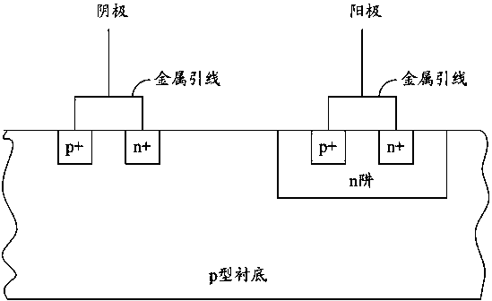
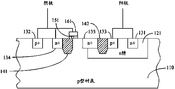
[0035] figure 2It is a schematic cross-sectional structure diagram of the first embodiment of the electrostatic discharge protection structure, including a p-type substrate 110 and an n-well 121 formed in the p-type substrate 110 by light doping. The n+ well region contact region 131 and the p+ well region anti-doping region 133 are formed by heavy doping in the n well 121, and the p+ substrate contact region 132 and n+ are formed by heavy doping in the p-type substrate 110 accordingly. The anti-doped region 134 of the substrate. The substrate anti-doping region 134 and the well region anti-doping region 133 are both located between the substrate contact region 132 and the well region contact region 131 .
[0036] Between the substrate anti-doping region 134 and the well region anti-doping region 133 , which is also the lateral junction between the p-type substrate 110 and the surface of the n well 121 , an n+ connection region 135 is formed by heavy doping. The connection ...
Embodiment 2
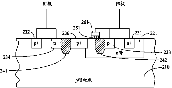
[0042] image 3 It is a schematic cross-sectional structure diagram of the second embodiment of the electrostatic discharge protection structure, and its structure and working principle are similar to those of the first embodiment. Specifically, the electrostatic discharge protection structure includes a p-type substrate 210 and an n-well 221 formed in the p-type substrate 210 by light doping. The n+ well region contact region 231 and the p+ well region anti-doping region 233 are formed by heavy doping in the n well 221, and the p+ substrate contact region 232 and n+ are formed by heavy doping in the p-type substrate 210 accordingly. The anti-doped region 234 of the substrate. The substrate anti-doping region 234 and the well region anti-doping region 233 are both located between the substrate contact region 232 and the well region contact region 231 .
[0043] Between the substrate anti-doping region 234 and the well region anti-doping region 233 , which is also the lateral...
Embodiment 3
[0048] Figure 4 It is a schematic cross-sectional structure diagram of the third embodiment of the electrostatic discharge protection structure, which is an embodiment after converting the n-well structure of the p-type substrate in the first embodiment into the p-well structure of the n-type substrate. It includes an n-type substrate 310 and a p-well 321 formed in the n-type substrate 310 by light doping. The p+ well region contact region 331 and the n+ well region anti-doping region 333 are formed by heavy doping in the p well 321, and the n+ substrate contact region 132 and p+ are formed by heavy doping in the n-type substrate 310 accordingly. The anti-doped region 334 of the substrate. The substrate anti-doping region 334 and the well region anti-doping region 333 are both located between the substrate contact region 332 and the well region contact region 331 .
[0049] Between the substrate anti-doping region 334 and the well region anti-doping region 333 , which is al...
PUM
 Abstract
Description
Claims
Application Information
 - R&D Engineer
- R&D Manager
- IP Professional
- Industry Leading Data Capabilities
- Powerful AI technology
- Patent DNA Extraction
Browse by: Latest US Patents, China's latest patents, Technical Efficacy Thesaurus, Application Domain, Technology Topic, Popular Technical Reports.
© 2024 PatSnap. All rights reserved.Legal|Privacy policy|Modern Slavery Act Transparency Statement|Sitemap|About US| Contact US: help@patsnap.com