


Quick Research
Generate reliable direction feasibility study reports for your R&D in just a few steps.

Technical Q&A
Discover and master advanced knowledge NOW. Basics, ideas, possibilities, all at once.

Find Solutions
As an expert in R&D theories, this can generate solutions to your technical problems instantly.

Evaluate Feasibility
Analyze your overall solution with one click, know your potential R&D risks in advance.

Monitor Landscape
Get weekly tech updates, stay abreast of the latest tech innovations and key insights.
Photovoltaic device, manufacturing method thereof, and photovoltaic module
A photovoltaic device and light-receiving surface technology, applied in photovoltaic power generation, final product manufacturing, sustainable manufacturing/processing, etc., can solve problems such as increased compound speed, reduced photovoltaic power, and reduced quality of semiconductor crystals, achieving ease of constraints, high photoelectricity Improve conversion efficiency and achieve cost reduction
- Summary
- Abstract
- Description
- Claims
- Application Information
AI Technical Summary
Problems solved by technology
Method used
Image

Examples
Embodiment approach
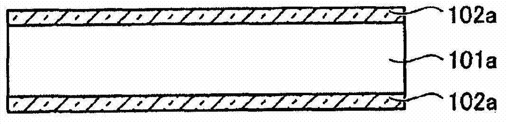
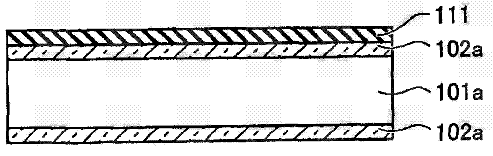
[0057] Below, refer to Figure 1-1 to Figure 1-10 as well as Figure 2-1 to Figure 2-10 , while following the manufacturing process, the embodiment of the present invention will be described. Figure 1-1 to Figure 1-10 It is a sectional view showing an example of a method of manufacturing a photovoltaic device according to an embodiment of the present invention. Figure 2-1 to Figure 2-10 It is a perspective view showing an example of a method of manufacturing a photovoltaic device according to an embodiment of the present invention. Figure 2-1 to Figure 2-10 The steps shown correspond to the Figure 1-1 to Figure 1-10 the steps shown.
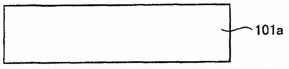
[0058] First, as a semiconductor substrate, for example, a p-type polysilicon substrate (hereinafter referred to as a p-type silicon substrate 101 a ) that is most widely used as a commercial solar cell is prepared ( Picture 1-1 , diagram 2-1 ).
[0059] The p-type silicon substrate 101a is produced by cutting and slicing a single-crys...
example 1
[0106] In the case of grid electrode spacing = 1 mm, process limit for patterning of high-concentration n-type diffusion layer = 100 μm (0.1 mm):
[0107] (0.1mm×0.1mm) / (1mm×1mm)=0.01(=1%)
[0108] (lower limit value example 2)
[0109] In the case of grid electrode spacing = 2 mm, process limit for patterning of high-concentration n-type diffusion layer = 100 μm (0.1 mm):
[0110] (0.1mm×0.1mm) / (2mm×2mm)=0.0025 (=0.25%)
[0111] In addition, in addition to the discontinuous shape, as the shape of the high-concentration n-type diffusion layer, a "wavy shape" that is continuous in the direction perpendicular to the longitudinal direction of the grid electrode in the light-receiving surface of the photovoltaic device and has a variable width is also proposed. "shape( Figure 9 ). Figure 9 It is a plan view schematically showing an example of the pattern of the high-concentration n-type diffusion layer 102a in this embodiment. exist Figure 9 middle, Figure 9 (a) shows a...
PUM
 Abstract
Description
Claims
Application Information
 - R&D Engineer
- R&D Manager
- IP Professional
- Industry Leading Data Capabilities
- Powerful AI technology
- Patent DNA Extraction
Browse by: Latest US Patents, China's latest patents, Technical Efficacy Thesaurus, Application Domain, Technology Topic, Popular Technical Reports.
© 2024 PatSnap. All rights reserved.Legal|Privacy policy|Modern Slavery Act Transparency Statement|Sitemap|About US| Contact US: help@patsnap.com