
Method for making patterning conducting layer

A technology for patterning conductive layers and conductive layers, which is applied in chemical/electrolytic methods to remove conductive materials, multilayer circuit manufacturing, and secondary processing of printed circuits, etc., which can solve problems such as complicated processes, difficult processes, and a lot of time spent , to achieve the effect of shortening the process time and simplifying the process steps

Inactive Publication Date: 2013-10-23
EFUN TECH CO LTD
View PDF0 Cites 1 Cited by
  • Summary
  • Abstract
  • Description
  • Claims
  • Application Information

AI Technical Summary

Problems solved by technology

[0005] The photolithographic etching process includes the steps of coating photoresist, covering photomask, exposing, removing photomask and developing, and removing photoresist. The steps are complicated and take a lot of time. What's more, the above-mentioned process has undergone two photolithography etchings in total, which makes the whole process too complicated and time-consuming
Moreover, when removing the second conductive layer 13 of the operating region 111 by the second photolithography etching, the second conductive layer 13 on the wiring region 112 must be shielded and protected, which also causes difficulty and complexity of the process.

Method used

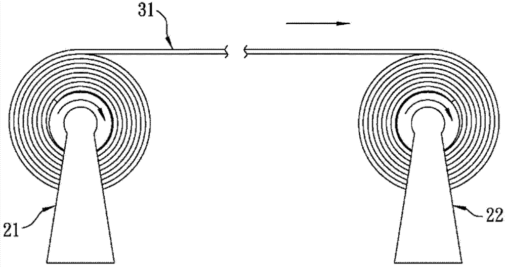
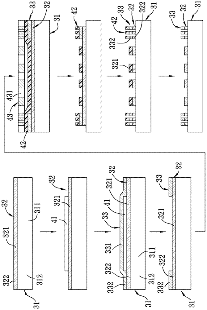

Image

  • Method for making patterning conducting layer
  • Method for making patterning conducting layer
  • Method for making patterning conducting layer

Examples


Embodiment Construction

[0024] In order to make the above objects, features and advantages of the present invention more comprehensible, specific implementations of the present invention will be described in detail below in conjunction with the accompanying drawings. First of all, it should be noted that the present invention is not limited to the following specific embodiments. Those skilled in the art should understand the present invention from the spirit embodied in the following embodiments, and each technical term can be optimized based on the spirit of the present invention. broad understanding. The same or similar components in the figures are denoted by the same reference numerals.

[0025] refer to figure 2 The method for making a patterned conductive layer in a preferred embodiment of the present invention is to coat a conductive film on the surface of a substrate 31 in conjunction with a roll-to-roll process, and etch the film into a predetermined pattern. The roll-to-roll process is t...


PUM


Abstract

Discloses is a method for making a patterning conducting layer, and the method comprises steps of: (A) draping a base material with a first conducting layer; (B) forming a layer of protective film on the surface of a first conducting zone of the first conducting layer; (C) draping with a second conducting layer, and the second conducting layer comprises a to-be-removed zone and a pattern-forming zone. (D) removing the protective film to expose the first conducting zone; (E) etching the pattern-forming zone of the second conducting layer and the first conducting layer to form a pattern. Before the second conducting layer is formed, the first conducting layer is shielded by the protective film at first, and then the protective film is removed so as to make the to-be-removed zone be removed together. In this way, only one time of photolithographic etching is capable of completing the making of two conducting layers, thereby simplifying processing steps and shortening processing time.

Description

technical field [0001] The invention relates to a method for making a patterned conductive layer, in particular to a method for plating at least two conductive layers on the surface of a base material and patterning the conductive layer. Background technique [0002] refer to figure 1 It is known that the plastic substrate 11 applied to electronic equipment, such as the substrate 11 of a touch panel, is usually coated with functional plastic on the surface of the substrate 11 in conjunction with a roll-to-roll process. Conductive thin film, and then etch the conductive thin film into the required pattern, as the electrode wire for transmitting the control signal. [0003] The specific manufacturing process is as follows: a layer of transparent first conductive layer 12 is plated on the surface of an operation area 111 and a wiring area 112 of the substrate 11 , and then a layer of second conductive layer 13 is plated. Since the operating area 111 is the operating area of ​...

Claims


Application Information

Patent Timeline
Patent Type & Authority Applications(China)
IPC IPC(8): H05K3/46H05K3/28H05K3/06
Inventor 傅绩惺王启任
Owner EFUN TECH CO LTD
Learn More