


Quick Research
Generate reliable direction feasibility study reports for your R&D in just a few steps.

Technical Q&A
Discover and master advanced knowledge NOW. Basics, ideas, possibilities, all at once.

Find Solutions
As an expert in R&D theories, this can generate solutions to your technical problems instantly.

Evaluate Feasibility
Analyze your overall solution with one click, know your potential R&D risks in advance.

Monitor Landscape
Get weekly tech updates, stay abreast of the latest tech innovations and key insights.
Semiconductor device and manufacturing method thereof
A manufacturing method and semiconductor technology, applied in semiconductor/solid-state device manufacturing, semiconductor devices, transistors, etc., can solve the problems of reduced device yield, reduced Schottky characteristics, difficult cleaning, etc., and achieve the effect of improving the cut-off withstand voltage
- Summary
- Abstract
- Description
- Claims
- Application Information
AI Technical Summary
Problems solved by technology
Method used
Image

Examples
no. 1 approach )
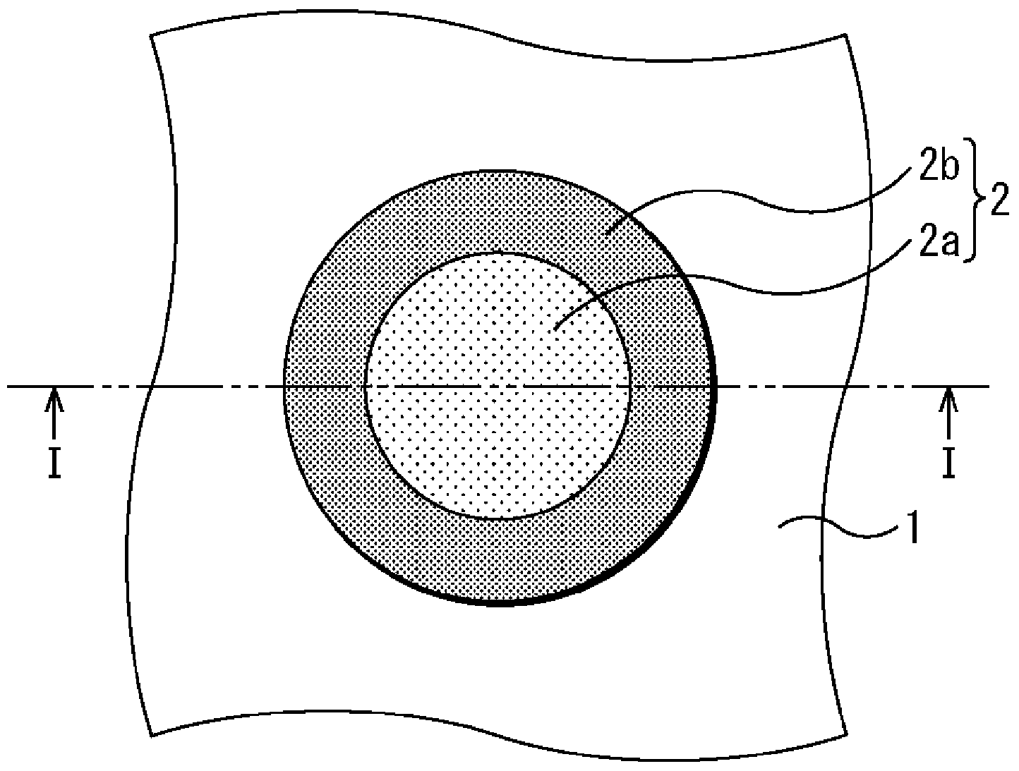
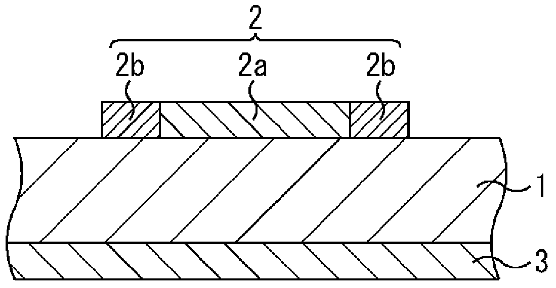
[0047] First, the first embodiment will be described. Figure 1A It is a plan view showing the structure of the semiconductor device (Schottky barrier diode) of the first embodiment, Figure 1B Is along Figure 1A A cross-sectional view of the line I-I.
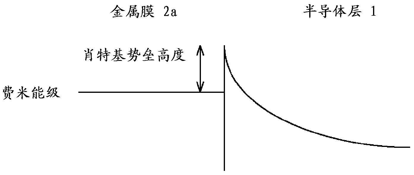
[0048] In the first embodiment, such as Figure 1A as well as Figure 1B As shown, a Schottky electrode 2 is formed on the semiconductor layer 1. In addition, an ohmic electrode 3 is formed on the back surface of the semiconductor layer 1. The Schottky electrode 2 includes a metal film 2a, which includes a metal Schottky bonded to the semiconductor layer 1, and a nitride film 2b, which is formed around the metal film 2a and is Schottky bonded to the semiconductor layer 1. The nitride film 2b contains the nitride of the metal contained in the metal film 2a. That is, the nitride film 2b contains a substance having a lower work function than the substance contained in the metal film 2a.
[0049] In the first embodiment configured in t...
no. 2 approach )
[0052] Next, the second embodiment will be described. Figure 3A Is a cross-sectional view showing the structure of the semiconductor device (Schottky barrier diode) of the second embodiment, showing the Figure 1A Section of the I-I line in.
[0053] In the second embodiment, such as Figure 2A As shown, a high-resistance region 4 is formed in a portion of the semiconductor layer 1 that is joined to the nitride film 2b. The resistance of the high-resistance region 4 is higher than the resistance of the portion of the semiconductor layer 1 joined to the metal film 2a. The other structure is the same as that of the first embodiment.
[0054] In the second embodiment configured in this way, since the high resistance region 4 exists, the diffusion of the depletion layer is greater when the reverse bias is applied. So like Figure 3B As shown, even if the Schottky barrier height is the same level as the first embodiment, the conduction band change in the high resistance region 4 and th...
no. 3 approach )
[0056] Next, the third embodiment will be described. Figure 4 It is a cross-sectional view showing the structure of a semiconductor device (Schottky barrier diode) of the third embodiment.
[0057] In the third embodiment, such as Figure 4 As shown, an n-type GaN layer 11b is formed on an n-type GaN substrate 11a. The GaN substrate 11a is doped 5×10 as n-type impurities, for example 17 cm -3 Si. The GaN layer 11b is doped 1×10 as an n-type impurity, for example 16 cm -3 Si. The thickness of the GaN layer 11b is, for example, about 1 μm. The GaN substrate 11 a and the GaN layer 11 b are contained in the semiconductor layer 11.
[0058] A passivation film 15 is formed on the GaN layer 11b. An opening 15a for the anode electrode is formed in the passivation film 15. As the passivation film 15, for example, a silicon nitride film having a thickness of about 400 nm is formed.
[0059] An anode electrode 12 (Schottky electrode) is formed in the opening 15a. The anode electrode 12 i...
PUM
| Property | Measurement | Unit |
|---|---|---|
| thickness | aaaaa | aaaaa |
| thickness | aaaaa | aaaaa |
| thickness | aaaaa | aaaaa |
Abstract
Description
Claims
Application Information
 - R&D Engineer
- R&D Manager
- IP Professional
- Industry Leading Data Capabilities
- Powerful AI technology
- Patent DNA Extraction
Browse by: Latest US Patents, China's latest patents, Technical Efficacy Thesaurus, Application Domain, Technology Topic, Popular Technical Reports.
© 2024 PatSnap. All rights reserved.Legal|Privacy policy|Modern Slavery Act Transparency Statement|Sitemap|About US| Contact US: help@patsnap.com