


Quick Research
Generate reliable direction feasibility study reports for your R&D in just a few steps.

Technical Q&A
Discover and master advanced knowledge NOW. Basics, ideas, possibilities, all at once.

Find Solutions
As an expert in R&D theories, this can generate solutions to your technical problems instantly.

Evaluate Feasibility
Analyze your overall solution with one click, know your potential R&D risks in advance.

Monitor Landscape
Get weekly tech updates, stay abreast of the latest tech innovations and key insights.
Semiconductor device
A semiconductor, conductive type technology, applied in the direction of semiconductor devices, semiconductor/solid-state device manufacturing, electrical components, etc., can solve the problems of increased switching loss, increased carrier concentration on the emitter side, etc., to achieve reduced switching loss, On-state voltage reduction effect
- Summary
- Abstract
- Description
- Claims
- Application Information
AI Technical Summary
Problems solved by technology
Method used
Image

Examples
no. 1 Embodiment approach
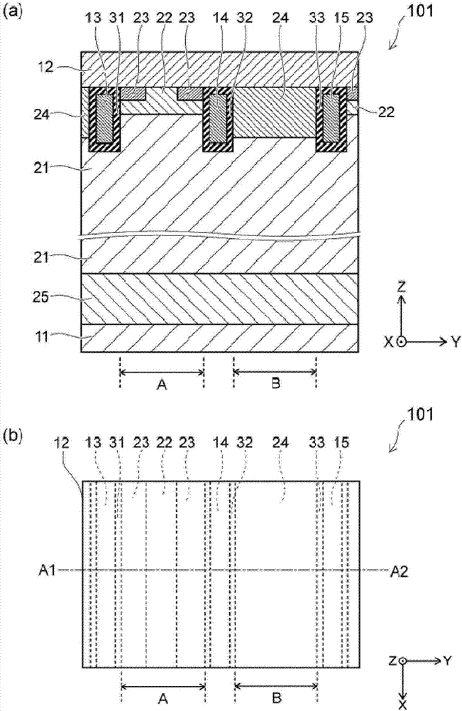
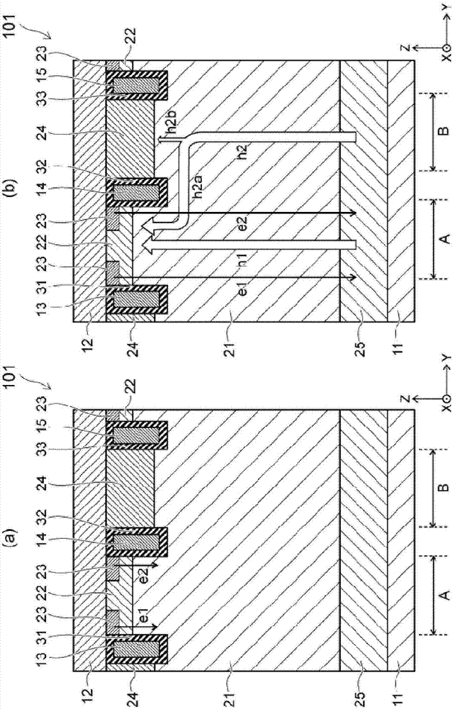
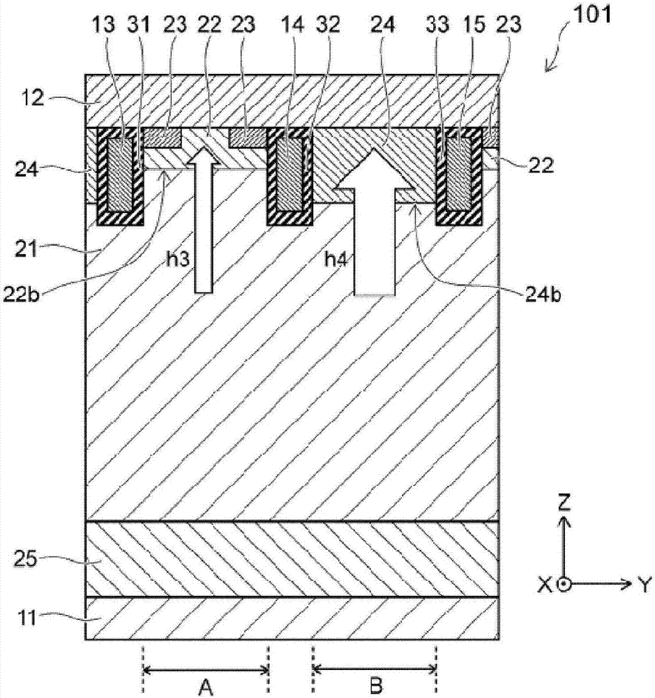
[0033] figure 1 (a) is a schematic cross-sectional view showing the semiconductor device according to the first embodiment. figure 1 (b) is a schematic plan view showing the semiconductor device of the first embodiment. exist figure 1 (a), shows along the figure 1 (b) A cross section of line A1-A2.
[0034] figure 1 The semiconductor device 101 shown in (a) is an IGBT having an upper and lower electrode structure. The semiconductor device 101 includes a first electrode (hereinafter, referred to as a collector electrode 11 , for example), a second electrode (hereinafter, referred to as an emitter electrode 12 , for example), a third electrode 13 , a fourth electrode 14 , a fifth electrode 15 , and a third electrode 13 . 1 semiconductor region (hereinafter, referred to as n - type base region 21), second semiconductor region (hereinafter, referred to as p-type base region 22, for example), third semiconductor region (hereinafter, referred to as n, for example, + type emit...
no. 2 Embodiment approach
[0078] Figure 4 It is a schematic cross-sectional view showing the semiconductor device of the second embodiment.
[0079] In the semiconductor device 102 , the length L24 of the p-type semiconductor region 24 is longer than the length L22 of the p-type base region 22 in the Y-axis direction. For example, the length of the A region is 1 μm or more and 6 μm or less. The length of the B region is 2 μm or more and 10 μm or less.
[0080] As a result, at the time of turning off, holes are more quickly discharged to the emitter electrode 12 via the wider p-type semiconductor region 24 . As a result, in the semiconductor device 102 , the switching loss at the time of turn-off is further reduced as compared with the semiconductor device 101 .
no. 3 Embodiment approach
[0082] Figure 5 (a) is a schematic cross-sectional view showing a semiconductor device according to a first example of the third embodiment. Figure 5 (b) is a schematic cross-sectional view showing a semiconductor device according to a second example of the third embodiment.
[0083] exist Figure 5 In the semiconductor device 103A shown in (a), n + The type emitter region 23 is provided on the side of the third electrode 13 and not provided on the side of the fourth electrode 14 . For example, n + The type emitter region 23 is in contact with the first insulating film 31 . n +The type emitter region 23 is not in contact with the second insulating film 32 . In addition, the fourth electrode 14 is electrically connected to the emitter electrode 12 . For example, the fourth electrode 14 is in contact with the emitter electrode 12 .
[0084] In addition, in the Y-axis direction, the p-type base region 22 is arranged in parallel with the p-type semiconductor region 24 wi...
PUM
 Abstract
Description
Claims
Application Information
 - R&D Engineer
- R&D Manager
- IP Professional
- Industry Leading Data Capabilities
- Powerful AI technology
- Patent DNA Extraction
Browse by: Latest US Patents, China's latest patents, Technical Efficacy Thesaurus, Application Domain, Technology Topic, Popular Technical Reports.
© 2024 PatSnap. All rights reserved.Legal|Privacy policy|Modern Slavery Act Transparency Statement|Sitemap|About US| Contact US: help@patsnap.com