Thin-film transistor substrate and manufacturing method

A technology of thin-film transistors and manufacturing methods, applied in the field of thin-film transistor substrates and their manufacturing, to achieve the effects of compact layout, excellent heat resistance, and increased aperture ratio

Active Publication Date: 2013-09-18
SHARP KK
View PDF4 Cites 3 Cited by
  • Summary
  • Abstract
  • Description
  • Claims
  • Application Information

AI Technical Summary

Problems solved by technology

It is also described that when heat treatment is performed at a high temperature of 350° C. or higher in order to restore the deteriorated electrical characteristics of the semiconductor layer, there is a possibility that the semiconductor layer reacts with the source electrode and the drain electrode to generate hillocks on the source electrode and the drain electrode ( unevenness), but since the deterioration of the electrical characteristics of the semiconductor layer can be suppressed even if heat treatment for forming a passivation film etc. is performed, heat treatment at 350° C. is not performed after forming the source electrode and the drain electrode

Method used


Image

  • Thin-film transistor substrate and manufacturing method
  • Thin-film transistor substrate and manufacturing method
  • Thin-film transistor substrate and manufacturing method

Examples


Embodiment approach 1

[0073] (Structure of liquid crystal display device)

[0074] -TFT Substrate-

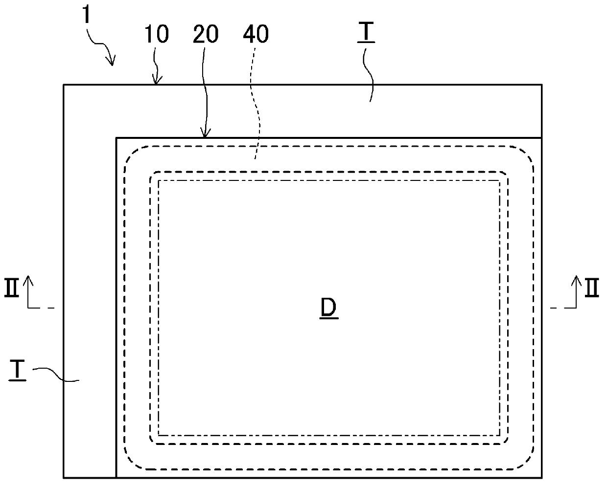
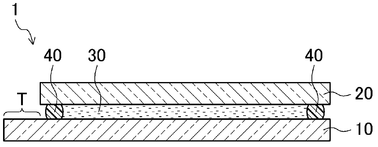
[0075] figure 1 It is a plan view of a liquid crystal display device 1 having a TFT substrate 10 of a thin film transistor according to Embodiment 1, figure 2 yes figure 1 Sectional view of line II-II. in addition, image 3 It is an enlarged plan view of the display area D of the TFT substrate 10 having the TFT of this embodiment, Figure 4 is an enlarged plan view of TFTs in the display region D of the TFT substrate 10, Figure 5 yes Figure 4 Cross-sectional view of the TFT at the V-V line.

[0076] In the liquid crystal display device 1 , a TFT substrate 10 and a counter substrate 20 are disposed so as to face each other, and both are bonded together by a sealing material 40 provided on the outer periphery of the substrates. Furthermore, in a region surrounded by the sealing material 40, a liquid crystal layer 30 is provided as a display medium layer.

[0077] In addition, in the liquid...

Embodiment approach 2

[0125] Next, a liquid crystal display device according to Embodiment 2 will be described.

[0126] -TFT Substrate-

[0127] In the liquid crystal display device 1 , as in Embodiment 1, the TFT substrate 10 and the counter substrate 20 are disposed so as to face each other, and both are adhered by the sealing material 40 provided on the outer peripheral edge of the substrates. In addition, a liquid crystal layer 30 is provided as a display medium layer in a region surrounded by the sealing material 40 .

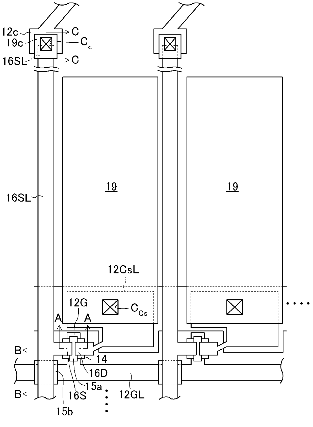
[0128] In addition, in the liquid crystal display device 1 , a display region D for image display is formed in a portion inside the sealing material 40 , and a terminal region T is formed in a portion protruding from the counter substrate 20 of the TFT substrate 10 .

[0129] TFT substrate 10, such as Figure 10 As shown, in the display area D, there are: a plurality of gate signal lines 12GL arranged to extend in parallel to each other; source signal lines 16SL; and a plur...


PUM


Abstract

The present invention prevents the formation of hillocks on source electrodes and drain electrodes during annealing at high temperatures of thin-film transistors provided with a channel protective layer. The source electrode (16S) and drain electrode (16D) on a thin-film transistor substrate, which has a channel protective film (15a) provided in islands so as to cover a channel part of an oxide semiconductor film (14), are constituted of an aluminum alloy film or a laminated film containing an aluminum alloy film.

Description

technical field [0001] The present invention relates to a thin film transistor substrate of a thin film transistor having an oxide semiconductor film, a display device, and a method for manufacturing the thin film transistor substrate. Background technique [0002] In general, as an active matrix substrate, a thin film transistor (Thin Film Transistor, hereinafter also referred to as "TFT") as a switching element is provided in each pixel as the smallest unit of an image (hereinafter also referred to as "TFT"). "TFT substrate") is widely used. [0003] A TFT with a general structure includes, for example: a gate electrode provided on an insulating substrate; a gate insulating film provided so as to cover the gate electrode; a semiconductor layer; and a source electrode and a drain electrode disposed opposite to each other on the semiconductor layer. [0004] The TFT substrate has a structure in which a plurality of TFTs are arranged in a matrix on the substrate, and an ins...

Claims


Application Information

Patent Timeline
Patent Type & Authority Applications(China)
IPC IPC(8): H01L29/786H01L21/28
CPCH01L29/66969H01L29/45H01L29/78606H01L29/78693
Inventor 加藤纯男
Owner SHARP KK
Why Eureka
Try Eureka