GaN-based LED and method for manufacturing GaN-based LED
A part, wet etching technology, applied in the direction of electrical components, circuits, semiconductor devices, etc., can solve problems such as falling off, affecting adhesion, dropping electrodes, etc., to achieve protection adhesion, enhanced adhesion, and increased firmness Effect
- Summary
- Abstract
- Description
- Claims
- Application Information
AI Technical Summary
Problems solved by technology
Method used
Image

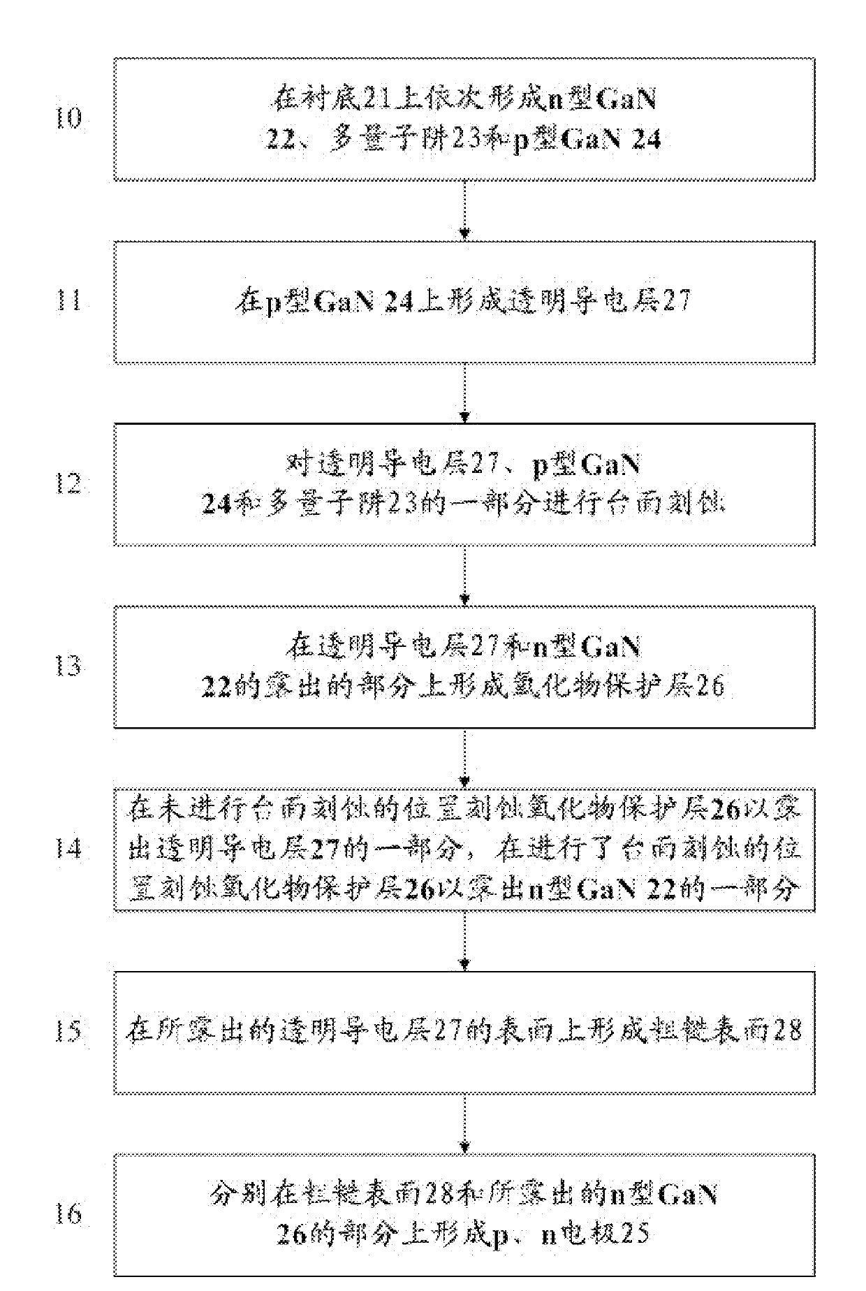
Examples
Embodiment Construction
[0034] Preferred embodiments of the present invention will be described in detail below with reference to the accompanying drawings, in which the same reference numerals denote the same elements.
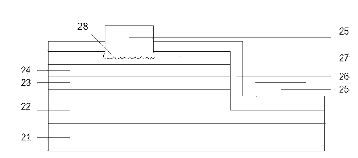
[0035] The purpose of the present invention is to treat the surface of the transparent conductive layer of the LED electrode to be evaporated by dry method or wet method to form a structure with a specific depth and surface roughness, thereby changing the contact between the electrode and the transparent conductive layer The form can effectively disperse the effect of external force on the transparent conductive layer and p-type gallium nitride when it is used by external force, reducing the probability and degree of electrode loss.
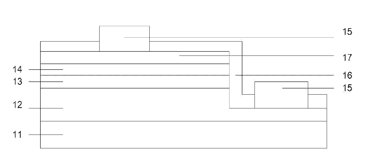
[0036] figure 2 is a method of manufacturing a GaN-based LED according to the present invention. image 3 is a schematic cross-sectional view of the structure of a GaN-based LED according to the present invention. Such as figure 2 and 3 As shown,...
PUM
 Abstract
Description
Claims
Application Information
 - Generate Ideas
- Intellectual Property
- Life Sciences
- Materials
- Tech Scout
- Unparalleled Data Quality
- Higher Quality Content
- 60% Fewer Hallucinations
Browse by: Latest US Patents, China's latest patents, Technical Efficacy Thesaurus, Application Domain, Technology Topic, Popular Technical Reports.
© 2025 PatSnap. All rights reserved.Legal|Privacy policy|Modern Slavery Act Transparency Statement|Sitemap|About US| Contact US: help@patsnap.com