Lithography illumination system

A lighting system and lithography technology, applied in microlithography exposure equipment, optics, optical components, etc., can solve the problem of low transmittance at the edge of the coated glass lens, affecting the uniformity of light intensity distribution, and uneven mask surface. Sensitivity and other issues, to avoid impact, strong practicability, and enhance the effect of light intensity

Active Publication Date: 2013-09-11
SHANGHAI MICRO ELECTRONICS EQUIP (GRP) CO LTD
View PDF8 Cites 7 Cited by
  • Summary
  • Abstract
  • Description
  • Claims
  • Application Information

AI Technical Summary

Problems solved by technology

If the deviation between the design telecentric value and the actual value is too large, the unevenness on the mask surface due to processing will be extremely sensitive, which will cause a great change in the imaging quality on the silicon wafer surface, especially the distortion
[0005] In the existing design, due to the limitation of coating conditions, the influence of the chamfering of the inte...

Method used


Image

  • Lithography illumination system
  • Lithography illumination system
  • Lithography illumination system

Examples


Embodiment Construction

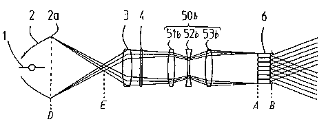
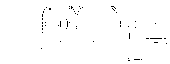
[0023] Specific embodiments of the present invention will be described in detail below in conjunction with the accompanying drawings. The specific structure of the lithography lighting system of the present invention is as follows: image 3 As shown, the illumination system includes: a high pressure mercury lamp 1 , a coupling lens group 2 , a quartz rod 3 , a relay lens group 4 and a mask plate 5 . The light emitted by the mercury lamp 1 is converged by the ellipsoid reflector and then incident on the incident end face 2a of the coupling lens group 2, the light beam is emitted from the outgoing end face 2b after being converged by the coupling lens group 2, and irradiates the incident end face 3a of the quartz rod 3, After the light beam undergoes multiple total reflections in the quartz rod 3, uniform illumination light is formed on the exit end face 3b of the quartz rod. The image is formed on the mask plate 5 , and a required illumination field of view with a certain nume...


PUM


Abstract

The invention provides a lithography illumination system which comprises a high-pressure mercury lamp, a coupled lens group, a quartz rod, a relay lens group and a mask plate, wherein light emitted from the mercury lamp is converged through the coupled lens group and forms uniform illuminating light in the quartz rod through repeated total reflection, and the illuminating light is amplified through the relay lens group and forms an illuminating view field with a certain numerical aperture, size and uniformity on the mask plate. The lithography illumination system is characterized in that the relay lens group is used for improving the illumination intensity of the edge field in the illuminating view field. Compared with the prior art, the lithography illumination system has the advantages that the illumination intensity of the edge field in the illuminating view field is improved, and the influence caused by the numerical aperture change of the mercury lamp is avoided, so that the mercury lamp light source and the whole illumination system have high practicality.

Description

technical field [0001] The invention relates to the field of integrated circuit equipment manufacturing, in particular to a lithography illumination system for a lithography device. Background technique [0002] Photolithography, also known as microlithography, is used to manufacture semiconductor devices and is an important process in semiconductor manufacturing. Many semiconductor devices can be fabricated by photolithography, such as diodes, triodes and integrated circuits. In the existing photolithography method, the optical system of high-pressure mercury lamp illumination is often used, mainly to expose the three lines of g (436nm) h (405nm) i (365nm), and transfer the pattern on the mask to the substrate (such as: silicon wafer) )superior. [0003] According to the requirements of photolithography production and exposure of semiconductor devices, the lighting system required by the lithography machine is usually required to be designed telecentrically. The light int...

Claims


Application Information

Patent Timeline
IPC IPC(8): G03F7/20G02B13/22G02B27/09
Inventor 周刚
Owner SHANGHAI MICRO ELECTRONICS EQUIP (GRP) CO LTD
Why Eureka
Try Eureka