LDMOS SCR for protection against integrated circuit chip ESD
A technology for integrated circuits and devices, applied in the field of LDMOS SCR devices for ESD protection of integrated circuit chips, can solve problems such as voltage reduction and device damage, and achieve the effects of process compatibility, enhanced ESD resistance, and improved latch-up immunity.
- Summary
- Abstract
- Description
- Claims
- Application Information
AI Technical Summary
Problems solved by technology
Method used
Image
Examples
specific Embodiment approach 1
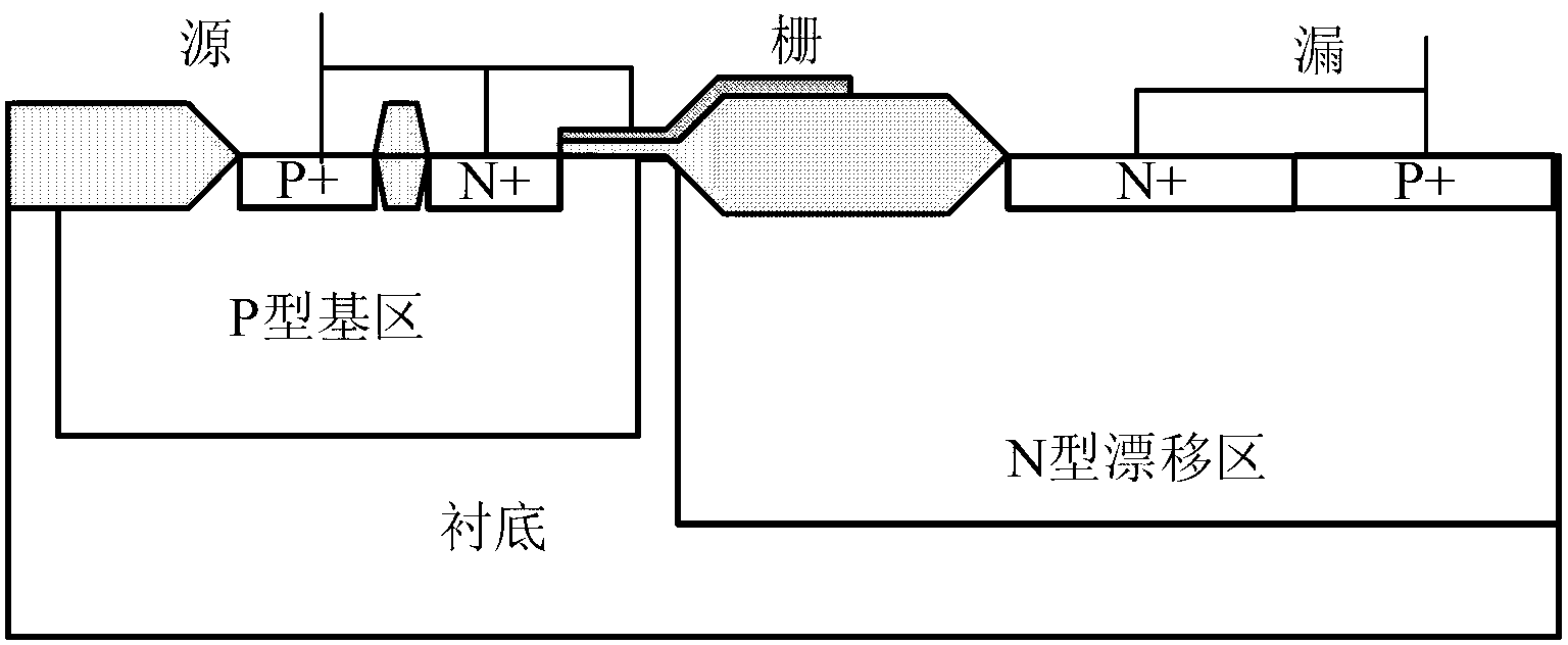
[0021] A kind of integrated circuit chip ESD protection LDMOS SCR device, such as image 3 As shown, it includes an nLDMOS device; the nLDMOS device includes an N-type drift region and a P-type base region located side by side on the substrate surface, wherein the N-type drift region and the P-type base region are in contact with each other or not; the P-type base region There is an N+ source region and a P+ contact region connected to the source metal in the region, wherein the N+ source region and the P+ contact region are in contact with each other or not; the side of the N-type drift region surface away from the P-type base region has a connection with the drain The metal-connected N+ drain region; the surface of the P-type base region between the N+ source region and the N-type drift region has a gate oxide layer, and the surface of the gate oxide layer has a polysilicon gate. The N-type drift region of the nLDMOS device also has a P well, and the existence of the P well ...
specific Embodiment approach 2
[0025] Such as Figure 5 shown, with image 3 Shown differently: simply put the figure 2 All the N-types in it are changed into P-type, and the P-type is changed into N-type, that is, the pLDMOS SCR device for ESD protection of integrated circuit chip provided by the present invention is obtained. The specific technical scheme is as follows:
[0026] A kind of integrated circuit chip ESD protection LDMOS SCR device, such as Figure 5As shown, it includes a pLDMOS device; the pLDMOS device includes a P-type drift region and an N-type base region located side by side on the substrate surface, wherein the P-type drift region and the N-type base region are in contact with each other or not; the N-type base region There is a P+ source region and an N+ contact region connected to the source metal in the region, wherein the P+ source region and the N+ contact region are in contact with each other or not; the side of the P-type drift region surface away from the N-type base region...
PUM
 Abstract
Description
Claims
Application Information
 - R&D
- Intellectual Property
- Life Sciences
- Materials
- Tech Scout
- Unparalleled Data Quality
- Higher Quality Content
- 60% Fewer Hallucinations
Browse by: Latest US Patents, China's latest patents, Technical Efficacy Thesaurus, Application Domain, Technology Topic, Popular Technical Reports.
© 2025 PatSnap. All rights reserved.Legal|Privacy policy|Modern Slavery Act Transparency Statement|Sitemap|About US| Contact US: help@patsnap.com


