Thin film transistor, manufacturing method of thin film transistor, array substrate and display device
A thin-film transistor and polysilicon technology, which is used in transistors, semiconductor/solid-state device manufacturing, and semiconductor devices, etc., can solve problems such as uneven etching and reduce process defect rates.
- Summary
- Abstract
- Description
- Claims
- Application Information
AI Technical Summary
Problems solved by technology
Method used
Image

Examples
Embodiment 1
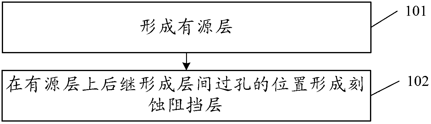
[0066] An embodiment of the present invention provides a method for manufacturing a thin film transistor, such as figure 2 and 3 As shown, the method includes:
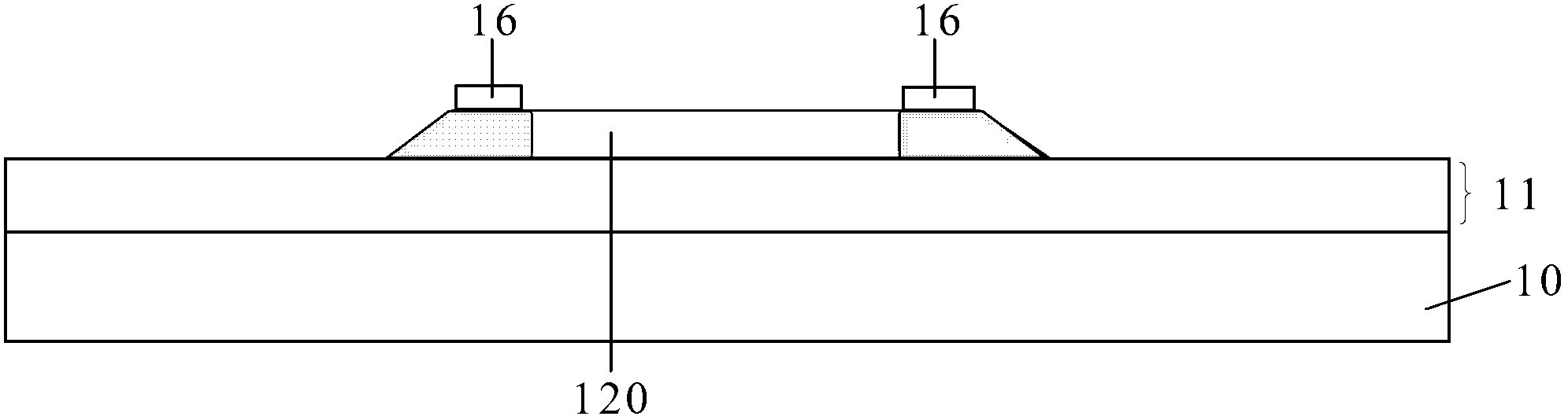
[0067] 101. Form an active layer 120, after forming the active layer 120, further include:
[0068] 102. Form an etching barrier layer 16 at the position where the interlayer via hole is subsequently formed on the active layer 120, so as to protect the active layer 120 when the interlayer via hole is etched. The interlayer via hole (not shown in the figure) Out) for connecting the active layer 120 and the source and drain electrodes (not shown in the figure).
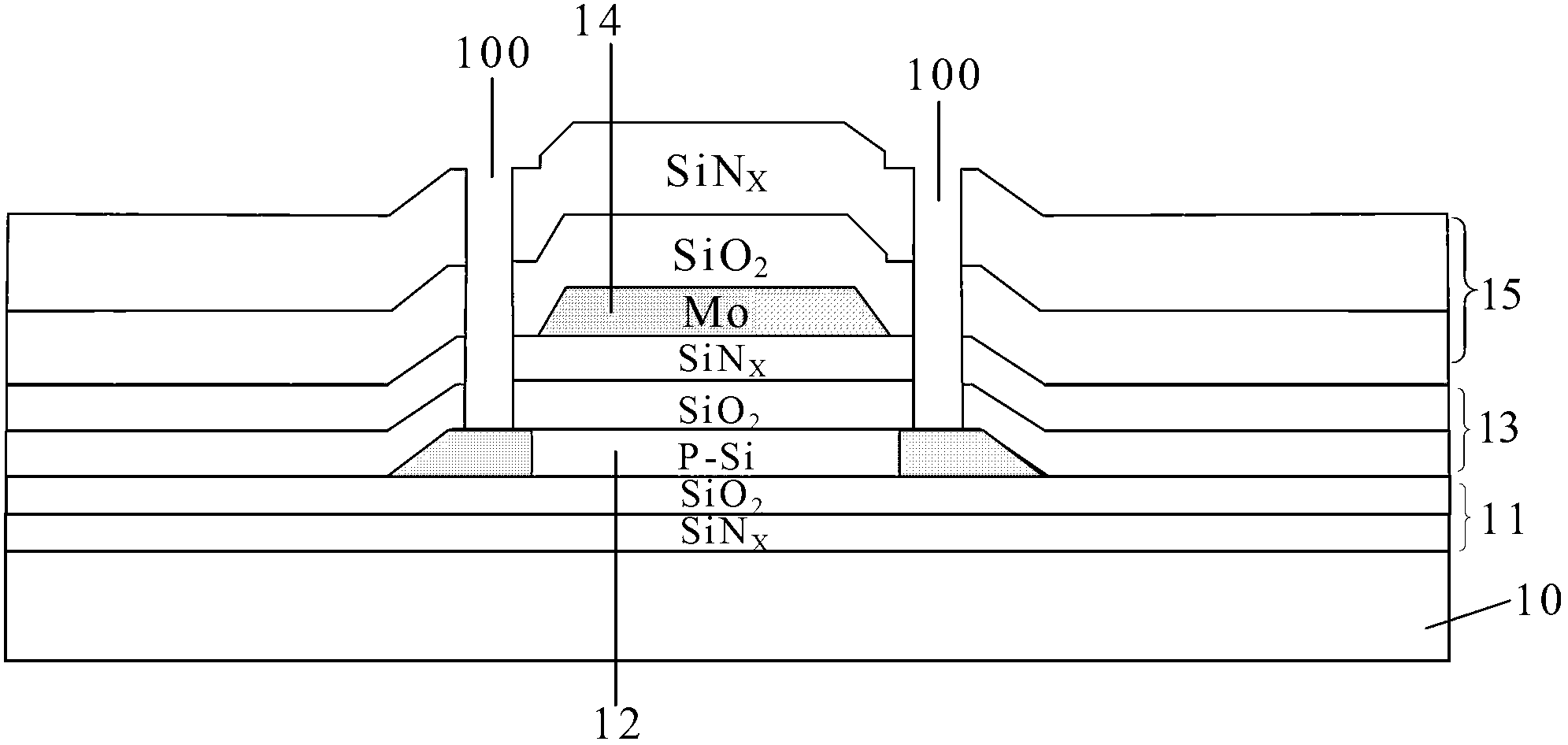
[0069] The interlayer via hole described in this embodiment is a via hole penetrating through all film layers between the active layer 120 and the source and drain electrodes, and the source electrode and the drain electrode pass through the doped region of the interlayer via hole and the active layer 120 respectively. electrical connection.
[0070] Prefe...
Embodiment 2
[0074] Further, the embodiment of the present invention also provides a thin film transistor manufacturing method, such as Figure 4 and Figure 5-7 As shown, the method specifically includes:
[0075] 201. Form a buffer layer 11 on a substrate 10;
[0076] 202. Form an amorphous silicon layer 121 on the buffer layer 11;
[0077] 203. Convert the amorphous silicon layer 121 into a polysilicon layer 122;
[0078] 204. Etching the polysilicon layer to form the active layer 12 of the TFT;
[0079] 205. Doping a part of the active layer 12 to form a semiconductor doped region;
[0080] Such as Figure 5 As shown, optionally, in steps 201-204, the buffer layer 11 and the amorphous silicon layer 121 are firstly deposited by chemical vapor deposition (PECVD), and then dehydrogenated, and then the amorphous silicon layer is deposited by excimer laser crystallization (ELA). The crystalline silicon layer 121 is converted into a polysilicon layer (P-Si) 122, and finally the active ...
Embodiment 3
[0094] Correspondingly, on the other hand, the present invention also provides a thin film transistor, comprising: an active layer, and further comprising:
[0095] An etch barrier layer used to protect the active layer when forming the interlayer via hole is arranged on the active layer at the position where the interlayer via hole is subsequently formed;
[0096] The interlayer vias are used to connect the active layer and the source and drain electrodes.
[0097] Further, the thin film transistor also includes:
[0098] a gate insulating layer disposed on the active layer and the etch stop layer;
[0099] a gate disposed on the gate insulating layer;
[0100] an interlayer insulating layer disposed on the gate;
[0101] The interlayer via hole penetrates through the interlayer insulating layer and the underlying gate insulating layer.
[0102] An embodiment of the present invention provides a thin film transistor. An etching stopper layer is provided on the active layer...
PUM
 Abstract
Description
Claims
Application Information
 - R&D
- Intellectual Property
- Life Sciences
- Materials
- Tech Scout
- Unparalleled Data Quality
- Higher Quality Content
- 60% Fewer Hallucinations
Browse by: Latest US Patents, China's latest patents, Technical Efficacy Thesaurus, Application Domain, Technology Topic, Popular Technical Reports.
© 2025 PatSnap. All rights reserved.Legal|Privacy policy|Modern Slavery Act Transparency Statement|Sitemap|About US| Contact US: help@patsnap.com