Method for detecting and representing morphology features of print of metal conducting wires on transparent base materials

A technology of metal wires and transparent substrates, applied in measuring devices, instruments, optical devices, etc., can solve problems such as deviation, reduction of electrical properties of wires and components, and achieve the effect of ensuring accuracy and improving resolution.

Inactive Publication Date: 2013-08-07
BEIJING INSTITUTE OF GRAPHIC COMMUNICATION
View PDF4 Cites 7 Cited by
  • Summary
  • Abstract
  • Description
  • Claims
  • Application Information

AI Technical Summary

Problems solved by technology

This deviation from the design in appearance often leads to the reduction or deviation of the electrical performance of the wire and the component device.

Method used


Image

  • Method for detecting and representing morphology features of print of metal conducting wires on transparent base materials
  • Method for detecting and representing morphology features of print of metal conducting wires on transparent base materials
  • Method for detecting and representing morphology features of print of metal conducting wires on transparent base materials

Examples


Embodiment Construction

[0044] In order to make the object, technical solution and effect of the present invention clearer, the present invention will be further described in detail below in conjunction with specific embodiments and with reference to the accompanying drawings.

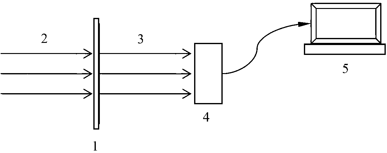
[0045] refer to figure 1 , is a schematic diagram of the optical path and main component units of the transmission image of the wire imprinted sample of the present invention. Including imprinted sample 1, vertical incident light 2 formed by illuminating white light path, transmitted light 3 formed after passing through imprinted sample, CCD imaging device 4, and computer and control software (computer control system) 5 connected to CCD device.

[0046] figure 1 The specific requirements and process of the detection and characterization of the metal wire imprint morphology features of the system shown are as follows:

[0047] The spectral energy distribution of the illuminating white light should be relatively balanced, and t...


PUM


Abstract

The invention relates to a method for detecting and representing morphology features of print of metal conducting wires on transparent base materials. The method includes (1), illuminating a sample from the back of the print sample of a metal conducting wire on a transparent base material along the direction perpendicular to the surface of the sample, and setting a CCD (charge coupled device) imaging system on the front surface of the print sample of the metal conducting wire on the transparent base material along the direction perpendicular to the surface of the sample; (2), calibrating the light transmittance of the CCD imaging system; (3), shooting to obtain grayscale digital images of print of the metal conducting wire on the transparent base material; (4), converting numerical values of the grayscale digital images by the aid of a calibration relation to form light transmittance digital images of the print sample; and (5), optionally selecting a section of the print of the metal conducting wire and acquiring morphology features such as the surface morphology, the surface roughness, the print line width and the line edge roughness of the print of the metal conducting wire by a technique for processing the digital images. A light source used in the step (1) supplies white parallel light. The method has the advantage that quantitative morphology parameters of the print of the metal conducting wire are acquired by the aid of transmission light information.

Description

technical field [0001] The invention relates to a method for detecting and characterizing the shape characteristics of metal wire imprints on a transparent substrate, which is used for detecting and characterizing the shape characteristics of nanometer metal wires formed by printing / printing on a transparent substrate, and for analyzing the characteristics of nanometer metal ink passing through. The printing / printing technology forms the shape quality of wire traces, and belongs to the technical field of printed electronics. Background technique [0002] Printed electronics technology is a production technology that uses printing technology to manufacture electronic product components. Its core idea is to formulate electronic materials into fluid "ink / ink" and print / print them into films, so as to obtain electronic products with lower production costs and raw material consumption. There are many types of printed electronic technologies, but generally meet the following char...

Claims


Application Information

Patent Timeline
Patent Type & Authority Applications(China)
IPC IPC(8): G01B11/24
Inventor 徐艳芳李路海李修李亚玲莫黎昕
Owner BEIJING INSTITUTE OF GRAPHIC COMMUNICATION
Why Eureka
Try Eureka