Dual-mode three-way wide-band filter based on multi-branch loaded square resonance ring
A technology of three-pass band and filter, which is applied in the direction of resonators, waveguide devices, electrical components, etc., can solve the problem of unsatisfactory frequency selectivity and achieve enhanced frequency selectivity and out-of-band suppression, enhanced frequency selectivity, The effect of downsizing
- Summary
- Abstract
- Description
- Claims
- Application Information
AI Technical Summary
Problems solved by technology
Method used
Image

Examples
Embodiment 1
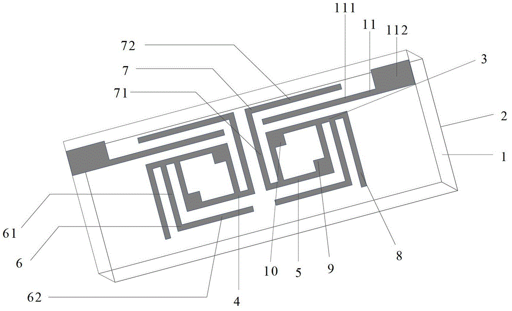
[0035] The structure of this embodiment is as figure 1 shown. It is mainly composed of a microstrip dielectric substrate 1, a metal ground plate 2, two symmetrical square resonant rings 3 and 4, and input and output feeders 11. Each square resonant ring includes a square metal ring 5 and upper perturbation branches 7 And the lower perturbation stub 6, the transmission zero stub 8 and a pair of perturbation metal sheets 9 and 10, wherein:
[0036] The microstrip dielectric substrate 1 adopts a single-sided copper-clad dielectric substrate with a dielectric constant of 2.65 and a thickness of 1 mm;
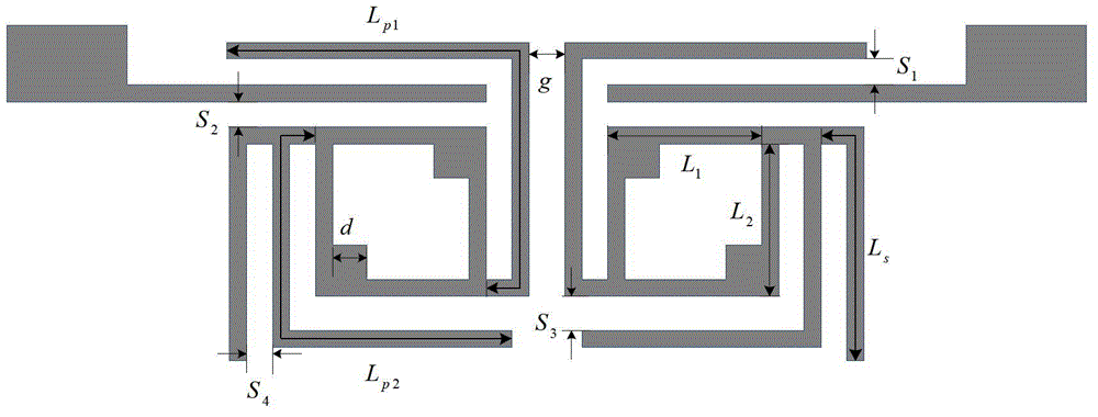
[0037] The lower layer of the microstrip dielectric substrate 1 is a copper-clad grounding plate 2. The square resonant rings 3 and 4 have the same structure and size, and are symmetrically located on the upper layer of the microstrip dielectric substrate 1. The microstrip line width of the square metal ring 5 is 0.4 mm. The circumference of square metal ring 5 is: 2 (L 1 +L 2 )...
Embodiment 2
[0045] The structure of this embodiment is the same as that of Embodiment 1, and the structural parameters different from Embodiment 1 are provided below:
[0046] The microstrip line width of the square metal ring 5 is 0.4mm, and the perimeter of the square metal ring 5 is: 2(L 1 +L 2 )=42.4mm, equal to a dielectric waveguide wavelength λ g , corresponding to the resonant frequency Among them, L 1 and L 2 is the length of the two sides of the square metal ring 5, and L 1 =12.8mm, L 2 =8.4mm, c is the speed of light in vacuum, ε e is the effective permittivity of the microstrip resonator, f 0 is the resonant frequency of the square metal ring 5;
[0047] The total length L of the upper perturbation stub 7 p1 =30.8mm, the length L of the lower perturbation stub 6 p2 =24.9mm, the line width of the upper perturbation branch 7 and the line width of the lower perturbation branch 6 are both 0.8mm, and the upper perturbation branch 7 and the lower perturbation branch 6 are...
Embodiment 3
[0053] The structure of the present embodiment is the same as that of embodiment 1, and the structural parameters different from embodiment 1 are provided below:
[0054] The microstrip line width of the square metal ring 5 is 0.8mm, and the perimeter of the square metal ring 5 is: 2(L 1 +L 2 )=41.2mm, which is equal to a dielectric waveguide wavelength λ g , corresponding to the resonant frequency Among them, L 1 and L 2 is the length of the two sides of the square metal ring 5, and L 1 =11.8mm, L 2 =8.8mm, c is the speed of light in vacuum, ε e is the effective permittivity of the microstrip resonator, f 0 is the resonant frequency of the square metal ring 5;
[0055] The total length L of the upper perturbation stub 7 p1 =25.8mm, the length L of the lower perturbation stub 6 p2 =25.7mm, the line width of the upper perturbation branch 7 and the line width of the lower perturbation branch 6 are both 0.4mm, and the upper perturbation branch 7 and the lower perturbat...
PUM
| Property | Measurement | Unit |
|---|---|---|
| Thickness | aaaaa | aaaaa |
| Frequency | aaaaa | aaaaa |
| Length | aaaaa | aaaaa |
Abstract
Description
Claims
Application Information
 - R&D
- Intellectual Property
- Life Sciences
- Materials
- Tech Scout
- Unparalleled Data Quality
- Higher Quality Content
- 60% Fewer Hallucinations
Browse by: Latest US Patents, China's latest patents, Technical Efficacy Thesaurus, Application Domain, Technology Topic, Popular Technical Reports.
© 2025 PatSnap. All rights reserved.Legal|Privacy policy|Modern Slavery Act Transparency Statement|Sitemap|About US| Contact US: help@patsnap.com