Electric, thermal and mechanical integrated design environment applicable to electronic product packaging design

A technology of electronic products and products, which is applied in special data processing applications, computing, electrical digital data processing, etc., can solve problems such as signal waveform distortion, interference, and delay generation, and achieve the effect of reducing complexity and design iterations

Inactive Publication Date: 2013-07-03
SHANGHAI RES INST OF MICROELECTRONICS SHRIME PEKING UNIV
View PDF0 Cites 5 Cited by
  • Summary
  • Abstract
  • Description
  • Claims
  • Application Information

AI Technical Summary

Problems solved by technology

When the operating frequency of the system is high, the wire interconnecting the devices should no longer be regarded as a simple wire transparent to the signa...

Method used


Image

  • Electric, thermal and mechanical integrated design environment applicable to electronic product packaging design

Examples


Embodiment Construction

[0010] In the following, an integrated design environment of electricity, heat and mechanics applied to packaging design of electronic products according to the present invention will be described in detail with specific examples in conjunction with the accompanying drawings.

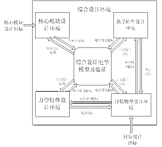
[0011] This embodiment provides an integrated design environment of electricity, heat and mechanics applied to packaging design of electronic products, figure 1 It is a schematic diagram of the realization of the present invention, including the core module design environment, the physical design environment of packaging, the thermal design environment of packaging, the electrical design environment of packaging, and the electrical simulation and verification environment of comprehensive design.

[0012] The core module design environment, according to the performance requirements of the product, carries out the design, simulation and verification of the core circuit of the electronic product and the des...


PUM


Abstract

The invention discloses a novel collaborative environment which contains electric, thermal and mechanical characteristics related to electronic product packaging. Compared with a conventional electronic product design, the design is greatly reduced in complexity on the aspects of a packaging method and a process, a product design period is shortened, and the success rate of a one-time design is increased. The environment is characterized in that the comprehensive, accurate and reconfigurable design parameters and performances and function prediction of the electronic product packaging are provided on an integrated design platform. By collaboratively considering the functions of packaging and thermal and mechanical characteristics on product performances, the product performance can be optimized through product core design optimization, packaging optimization, thermal optimization and mechanical design optimization according to the design cost and implementation complexity in a product design stage. On the one hand, the product performances are realized through low cost, and on the other hand, the freedom of a plurality of designs is provided, so that the performance implementation complexity is lowered; and most important of all, the expectation of the product performances can be accurately estimated in a product design stage, so that design iteration is reduced.

Description

technical field [0001] The invention relates to the fields of packaging design for electronic circuits, automation of electronic circuit design, and computer aided design of electronic circuits. Background technique [0002] With the continuous advancement of electronic technology and integrated circuit technology, the clock rate of digital systems is getting higher and higher, and the signal edge rate is getting faster and faster. From the perspective of electrical performance, the interconnection between high-speed signals is no longer smooth and transparent. The impact of PCB wire interconnection and board layer characteristics on the system can no longer be simply ignored. There are gold wires, metal wires on the substrate, vias and corners, stubs, solder balls, etc. in the package interconnection. In low-frequency signals, they are often regarded as simple transmission lines. When the operating frequency of the system is high, the wire interconnecting the devices shoul...

Claims


Application Information

Patent Timeline
IPC IPC(8): G06F17/50
Inventor 刘少龙程玉华
Owner SHANGHAI RES INST OF MICROELECTRONICS SHRIME PEKING UNIV
Why Eureka
Try Eureka