
Opposite electrode structure, SiC photoconductive semiconductor switch (PCSS) and manufacturing methods thereof

A technology of electrode structure and photoconductive switch, which is applied in the direction of final product manufacturing, sustainable manufacturing/processing, and circuits, and can solve the problems of small light-transmitting area and large on-resistance

Active Publication Date: 2013-06-26
SHANGHAI INST OF CERAMIC CHEM & TECH CHINESE ACAD OF SCI
View PDF6 Cites 12 Cited by
  • Summary
  • Abstract
  • Description
  • Claims
  • Application Information

AI Technical Summary

Problems solved by technology

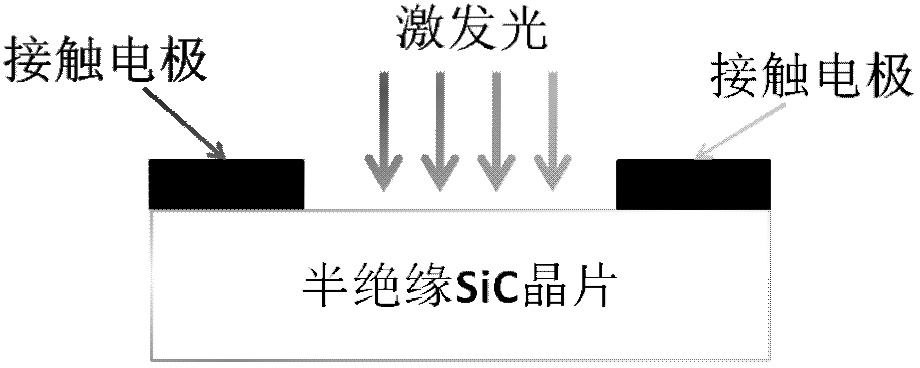
However, since the excitation light is incident through the side of the substrate, the light transmission area is small and the on-resistance will be large.

Method used


Image

  • Opposite electrode structure, SiC photoconductive semiconductor switch (PCSS) and manufacturing methods thereof
  • Opposite electrode structure, SiC photoconductive semiconductor switch (PCSS) and manufacturing methods thereof
  • Opposite electrode structure, SiC photoconductive semiconductor switch (PCSS) and manufacturing methods thereof

Examples


Embodiment 1

[0042] Embodiment 1 (the present invention)

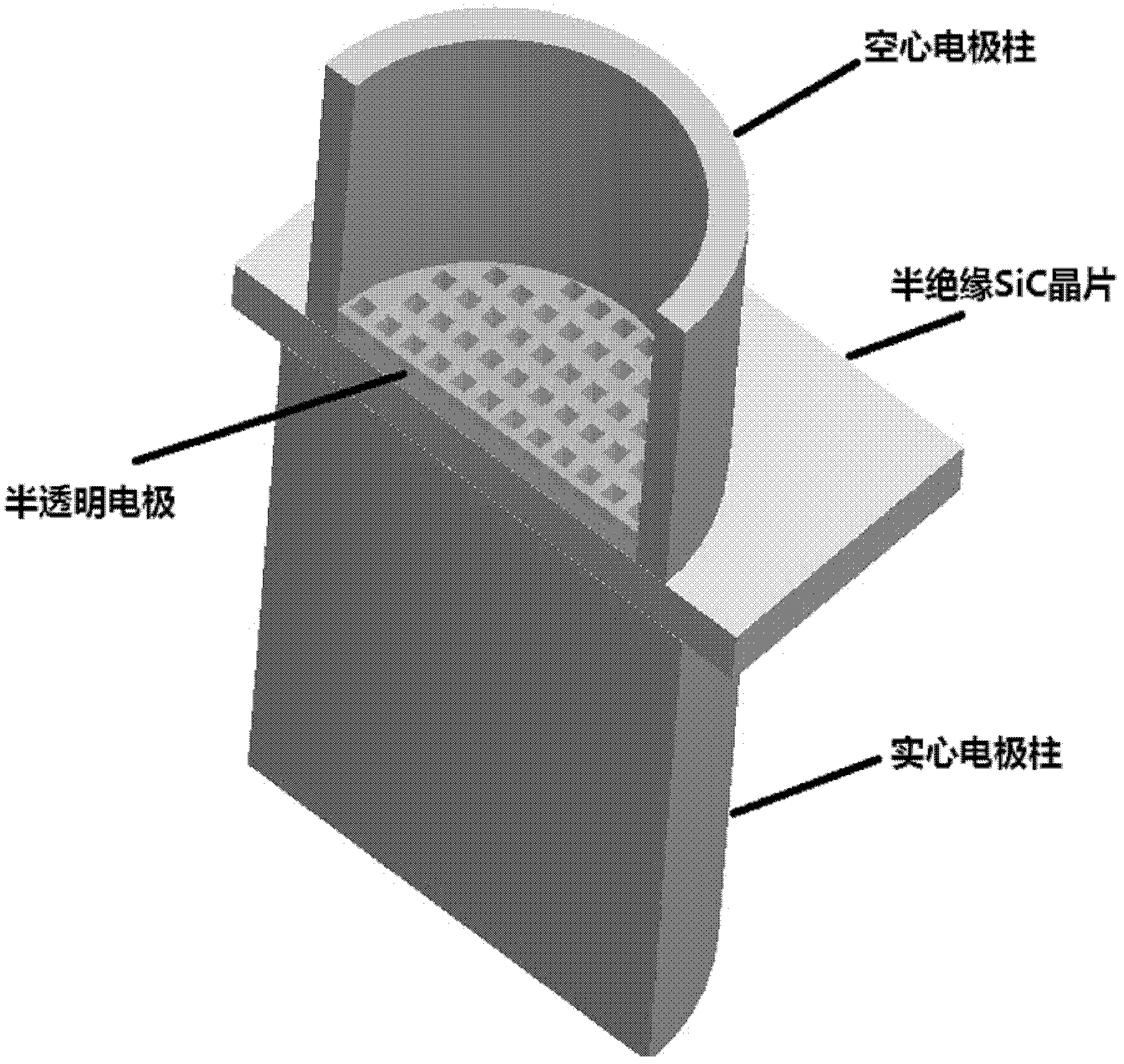
[0043] A semi-insulating SiC wafer with a (11-20) plane is used, and the wafer is polished using the method described in step (2). After polishing, the thickness of the wafer is 0.4 mm. Wafers were cut into 1.2 cm x 1.2 cm square pieces and cleaned using RCA standard processes. One side of the wafer is plated with Au(500nm) / Pt(100nm) / Ti(100nm) / Ni(50nm) electrodes, the electrodes are circular with a diameter of 10mm, and are rapidly annealed in an Ar atmosphere at an annealing temperature of 1000°C. Annealing time 2 minutes. On the other side of the wafer, a semi-transparent Au(500nm) / Pt(100nm) / Ti(100nm) / Ni(50nm) electrode is plated using a mold, and the electrode is a circle of 8mm. A solid Al electrode post with a diameter of 10 mm is welded to the front side of the wafer, and a hollow Al electrode post with an inner diameter of 7 mm and an outer diameter of 8 mm is welded to the reverse side of the wafer. The switch is encapsu...

Embodiment 2

[0045] Embodiment 2 (comparison)

[0046] A semi-insulating SiC wafer with a (11-20) plane is used, and the wafer is polished using the method described in step (2). After polishing, the thickness of the wafer is 0.4 mm. Wafers were cut into 1.2 cm x 1.2 cm square pieces and cleaned using RCA standard processes. Both sides of the wafer are coated with Au(500nm) / Pt(100nm) / Ti(100nm) / Ni(50nm) electrodes, the electrodes are circular with a diameter of 10mm, and are rapidly annealed in an Ar atmosphere at an annealing temperature of 1000°C. Annealing time 2 minutes. Solid Al electrode posts with a diameter of 10 mm were welded to the front and back of the wafer. The switch is encapsulated using a Teflon mold. The packaging material uses epoxy polymer insulating material, mixed with 15% BaTiO 3 , Under 0.5Pa air pressure, degas the encapsulated switch to extract the air bubbles in the encapsulation material.

[0047] Excited with 532nm light, the energy is 5mJ per pulse, and th...


PUM

PropertyMeasurementUnit
Surface roughnessaaaaaaaaaa

Abstract

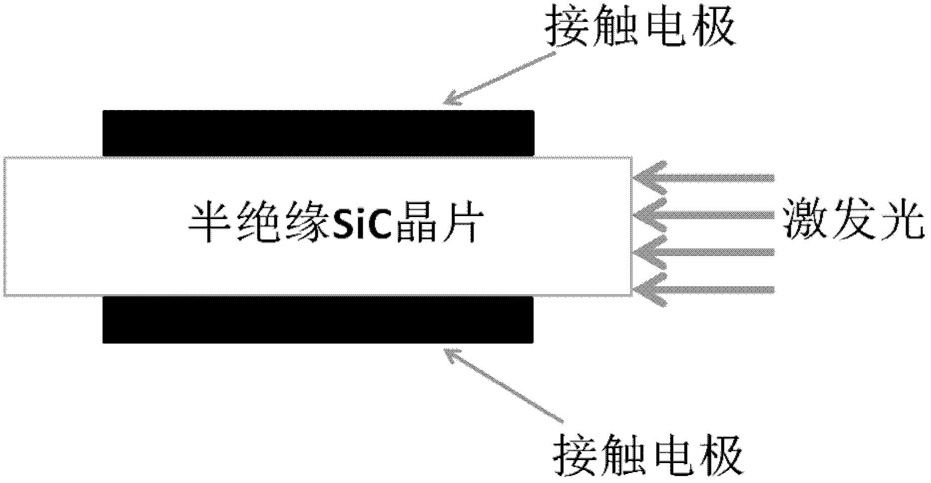
The invention belongs to the field of semiconductor devices and relates to an opposite electrode structure, an SiC photoconductive semiconductor switch (PCSS) and manufacturing methods thereof. The opposite electrode structure comprises a semi-insulating SiC wafer, a hollow electrode post, a semitransparent or transparent electrode layer and a solid electrode post, wherein the semi-insulating SiC wafer is a high-purity semi-insulating or vanadium doped semi-insulating SiC wafer which is subjected to polishing treatment; the semitransparent or transparent electrode layer is an Au (500nm) / Pt (100nm) / Ti (100nm) / Ni (50nm) semitransparent electrode structure or a transparent conducting thin film, and the Au (500nm) / Pt (100nm) / Ti (100nm) / Ni (50nm) semitransparent electrode structure or the transparent conducting thin film is optionally selected for corresponding annealing; and the hollow electrode post and the solid electrode post are preferably a hollow aluminum electrode post and a solid aluminum electrode post respectively. The SiC PCSS is obtained by subjecting the opposite electrode structure to insulating package and air pumping package by using a Teflon mould. Compared with SiC photoconductive semiconductor switches in prior art, the SiC PCSS has the advantages that light pass areas can be increased, and simultaneously, high withstand voltage of the PCSS can be guaranteed.

Description

technical field [0001] The invention belongs to the field of semiconductor devices, and relates to a novel positive-opposite electrode structure and a manufacturing method thereof. In addition, the present invention also relates to a SiC photoconductive switch comprising the novel facing electrode structure and a manufacturing method thereof. Background technique [0002] The full name of photoconductive switch is Optically Controlled Photoconductive Semiconductor Switches (PCSS), which is a new type of switching device formed by combining an ultrafast pulse laser and a photoconductor (such as GaAs, InP, SiC, etc.). Its working principle is to use ultrashort laser pulses to generate electron-hole pairs in semiconductor materials to realize the control of the conductivity of the material, that is, to control the closure of the switch. Compared with traditional switches, it has the advantages of simple structure, fast response, stable trigger, no trigger jitter, large dynamic...

Claims


Application Information

Patent Timeline
IPC IPC(8): H01L31/0224H01L31/18H01L31/08
CPCY02P70/50
Inventor 常少辉黄维刘学超杨建华施尔畏
Owner SHANGHAI INST OF CERAMIC CHEM & TECH CHINESE ACAD OF SCI
Learn More