Inductor

一种电感器、配线的技术,应用在电感器领域,能够解决半导体集成电路成本上升、半导体集成电路面积变大等问题,达到增加自由度、增强频带扩展效果的效果

Inactive Publication Date: 2013-06-19
NIPPON TELEGRAPH & TELEPHONE CORP +1
View PDF5 Cites 2 Cited by
  • Summary
  • Abstract
  • Description
  • Claims
  • Application Information

AI Technical Summary

Problems solved by technology

However, the area of ​​the inductor is much larger than that of the transistor, the area of ​​the semiconductor integrated circuit becomes larger, and the cost of the semiconductor integrated circuit rises

Method used


Image

  • Inductor
  • Inductor
  • Inductor

Examples


no. 1 approach

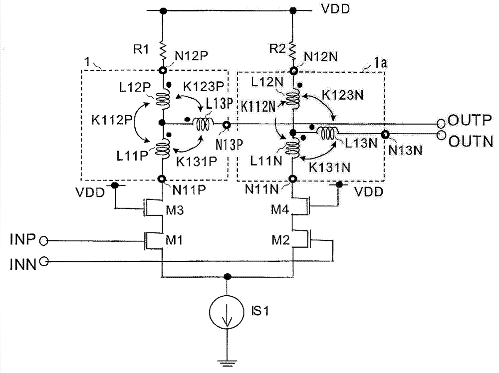
[0030] Now, embodiments of the present invention will be described below with reference to the drawings. figure 1 is a plan view of the inductor according to the first embodiment of the present invention. figure 2 is along figure 1 Cross-sectional view of an inductor along line A-A. notice, figure 1 A plurality of metal wiring layers are shown in perspective. refer to figure 1 , the inductor 1 according to the present embodiment includes a first shunt inductor L11P (first inductor wiring), a second shunt inductor L12P (second inductor wiring), and a first series inductor L13P (second inductor wiring). three inductor wiring).

[0031] A rectangular or circular area in which the inductors L11P, L12P, and L13P are formed is hereinafter referred to as an inductor area. exist figure 1 In the example shown in , the area indicated by the dashed line is the inductor area.

[0032] The first shunt inductor L11P is formed using the first metal wiring layer 30 . The first ...


PUM


Abstract

An inductor (1) is provided with: inductor (L11P), the start point of which is connected to terminal (N11P), and which is formed in the shape of a spiral on the outer circumference of an inductor region; inductor (L12P), the end point of which is connected to terminal (N12P), and which is formed in the shape of a spiral on the inner circumference of the inductor region with the end point of inductor (L11P) functioning as the start point of inductor (L12P); and inductor (L13P), the end point of which is connected to terminal (N13P), and which is formed in the shape of a spiral in a region sandwiched by inductor (L11P) and inductor (L12P) with the connecting point of inductor (L11P) and inductor (L12P) functioning as the start point of inductor (L13P).

Description

technical field [0001] The present invention relates to an inductor that is mainly applicable to an inductor formed using a metal wiring layer in a semiconductor integrated circuit that handles high-frequency signals, such as a transconductor used in a light receiving module. An amplifier or a laser driving circuit used in an optical transmitting module, and more particularly, the present invention relates to an inductor which is indispensable in a peaking circuit for realizing a high frequency response. Background technique [0002] Silicon CMOS transistors have the advantages of ensuring a high degree of integration and being able to provide semiconductor integrated circuits inexpensively through mass production. On the other hand, since the cutoff frequency of the silicon CMOS transistor is lower than that of a transistor using a compound semiconductor represented by InP, the operating frequency of the circuit becomes lower. To solve this problem, a technique is widely u...

Claims


Application Information

Patent Timeline
Patent Type & Authority Applications(China)
IPC IPC(8): H01L21/822H03F3/45H01L27/04
CPCH01L23/5227H01L28/10H03F3/195H03F3/45188H03F2203/45731H01L2924/0002H03F1/565H01L2924/00H01F27/2804H01F27/29H03H11/02
Inventor 大友祐辅桂井宏明小野寺秀俊土谷亮
Owner NIPPON TELEGRAPH & TELEPHONE CORP
Why Eureka
Try Eureka