
OLED (organic light-emitting diode) display

A display and touch electrode technology, which is applied in the field of OLED displays, can solve the problems of complex module manufacturing process, increasing the thickness of touch electrodes and touch electrode protective films, which is not conducive to the thinning of the display, and achieve the goal of simplifying the process and reducing the thickness Effect

Inactive Publication Date: 2013-04-17
NANJING CEC PANDA LCD TECH
View PDF4 Cites 36 Cited by
  • Summary
  • Abstract
  • Description
  • Claims
  • Application Information

AI Technical Summary

Problems solved by technology

The display with this structure requires two substrates to complete the display and touch functions, making the module manufacturing process more complicated
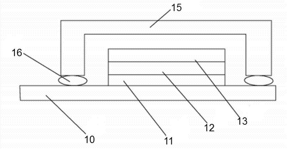
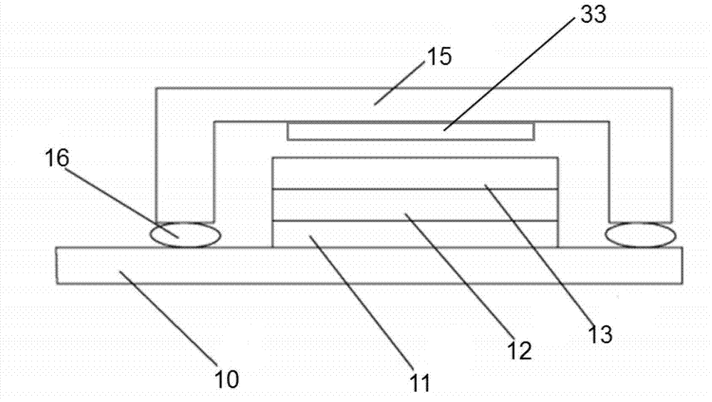
At the same time, the box body formed by the OLED substrate 11 and the packaging glass 15 increases the thickness of the touch electrodes and the touch electrode protective film, which is not conducive to the thinning requirements of the display.

Method used


Image

  • OLED (organic light-emitting diode) display
  • OLED (organic light-emitting diode) display
  • OLED (organic light-emitting diode) display

Examples


Embodiment Construction

[0024] Below in conjunction with accompanying drawing and specific embodiment, further illustrate the present invention, should be understood that these embodiments are only for illustrating the present invention and are not intended to limit the scope of the present invention, after having read the present invention, those skilled in the art will understand various aspects of the present invention Modifications in equivalent forms all fall within the scope defined by the appended claims of this application.

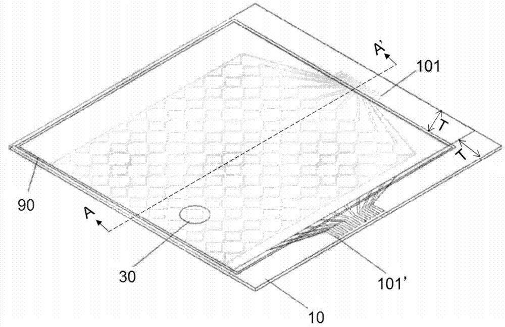
[0025] In the OLED display integrated with the touch function provided by the present invention, electrodes with the touch function and OLED light-emitting elements are arranged on the same substrate. See eg image 3 It is the first embodiment of the present invention. As shown in the figure, an insulating layer (not shown) is provided on a prior art substrate 10 with OLED light-emitting elements, wherein the substrate 10 is divided into a pixel area P (not shown) and a...


PUM


Abstract

The invention discloses an OLED (organic light-emitting diode) display, which comprises a base plate, an isolation layer and a touch controlled functional layer, wherein an OLED light-emitting element is formed on the base plate. The OLED light-emitting element comprises an OLED displaying component, an organic light-emitting functional layer and an OLED anode; the isolation layer is formed on the OLED light-emitting element; the touch controlled functional layer is formed on the isolation layer, and the touch controlled functional layer is provided with a touch controlled electrode; and the touch controlled electrode and the OLED anode are respectively connected onto respective ICs (integrated circuits) to form a top light-emitting OLED display integrated with touch control. A shielding layer is arranged between the isolation layer and the touch controlled functional layer, an insulation layer is arranged on the shielding layer, and thus signal interference between the OLED light-emitting element and the touch controlled functional layer is prevented. As the OLED light-emitting element and the touch controlled functional layer are arranged on the same base plate, the thickness of the OLED display integrated with a touch control function in the prior art is reduced. The touch controlled electrode is connected onto the terminal part of the base plate and is further connected onto the respective IC through the terminal part, thus the manufacture process of the display is simplified.

Description

technical field [0001] The invention relates to the technical field of OLED displays, in particular to an OLED display with an integrated touch function. Background technique [0002] The display integrated touch technology that controls the display through induction has been widely used in display devices such as mobile phones and tablet computers. Organic electroluminescent displays, OLED (Organic Light-Emitting Diode), are known for their active light emission, high contrast, and With many advantages such as fast response speed and thinness, it is known as a new generation of displays that can replace liquid crystal displays (LCDs). And an OLED display with integrated functions is the mainstream of existing touch-sensitive displays. [0003] Schematic diagram of the structure of an OLED display figure 1 As shown, it includes an OLED substrate 10 , a cathode 11 that is a common electrode, an organic light-emitting functional layer 12 , an anode 13 that is a transparent e...

Claims


Application Information

Patent Timeline
IPC IPC(8): H01L27/32G06F3/044
Inventor 洪孟逸
Owner NANJING CEC PANDA LCD TECH
Learn More