Display device

A technology for display devices and display parts, which is applied to identification devices, static indicators, instruments, etc., can solve the problems of inability to represent display transistors, inability to represent multiple transistors, and inability to monitor the process of loading and unloading protective films, and achieves the effect of strengthening static electricity.

Active Publication Date: 2013-04-17
SAMSUNG DISPLAY CO LTD
View PDF8 Cites 6 Cited by
  • Summary
  • Abstract
  • Description
  • Claims
  • Application Information

AI Technical Summary

Problems solved by technology

[0005] However, the transistors inside the test element group are independent transistors, which cannot represent the overall connection of multiple transistors inside the display area.
Therefore, even if the transistors in the test element group are degraded by static electricity, the transistors in the display area can be driven normally, so there is a disadvantage that the transistors in the test element group cannot represent the transistors in the display area
[0006] As mentioned above, since the transistors inside the test element group are independent structures, it is impossible to monitor the protective film loading and unloading process, film scribing (scribing) process, laser lift off (Laser Lift Off, LLO for short) process and mold process of flexible display devices. Static electricity generated during the module process, etc.

Method used


Image

  • Display device
  • Display device
  • Display device

Examples


Embodiment Construction

[0042] Hereinafter, embodiments of the present invention will be described with reference to the drawings so that those skilled in the art to which the present invention pertains can easily implement the present invention. The present invention can be implemented in various forms and is not limited to the embodiments described here.

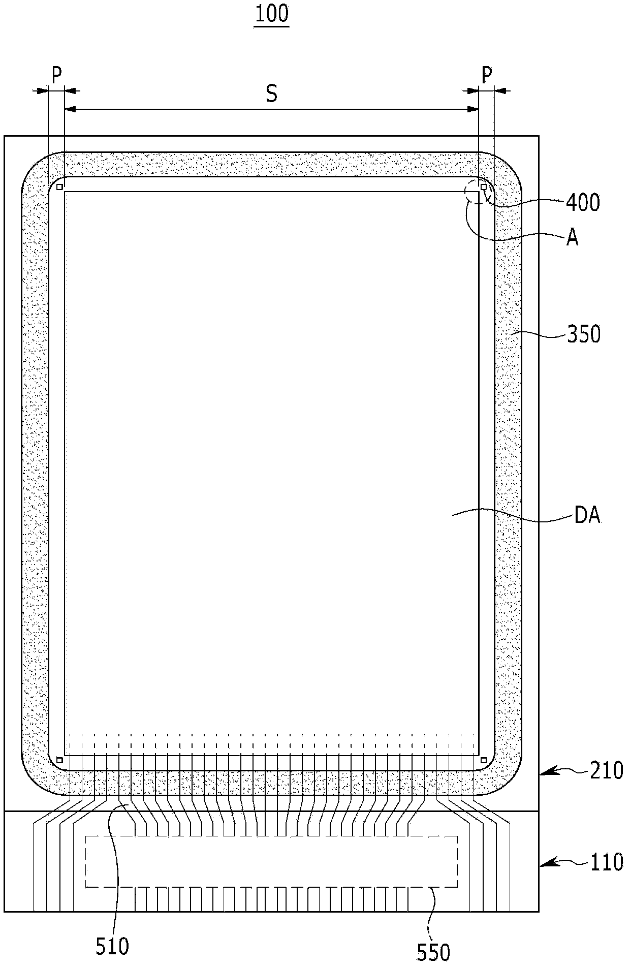
[0043] figure 1 is a plan view of a display device according to a first embodiment of the present invention, figure 2 yes figure 1 A magnified view of part A of .

[0044] Such as figure 1 As shown, the display device 100 according to the first embodiment of the present invention includes: a display substrate 110 ; a sealing member 210 covering the display substrate 110 ; and a sealant 350 disposed between the display substrate 110 and the sealing member 210 .

[0045] The sealant 350 is disposed along the edge of the sealing member 210 , and the sealant 350 makes the display substrate 110 and the sealing member 210 adhere and seal together....


PUM


Abstract

A display device according to an exemplary embodiment of the present invention includes a display portion including a plurality of display pixels displaying an image and a dummy portion including a plurality of dummy pixels formed in a periphery region of the display portion. An electrostatic test element group (TEG) may be formed in at least one of the dummy pixels.

Description

technical field [0001] The present invention relates to a display device, and more particularly to a display device for displaying images. Background technique [0002] In order to confirm whether the implementation results of each process of manufacturing the display device have reached a better state, it is necessary to measure the thickness, resistance, concentration, degree of contamination, critical value, and electrical characteristics of the device of each process result. Due to damage to the device, process characteristics may not be monitored on the actual substrate. [0003] In this case, a pattern called a Test Element Group (TEG) is formed on a specific portion of the substrate on which the device is formed or in another blank area and similarly performed on the substrate on which the actual device is formed. After the process performed on the substrate, the test element set is measured to evaluate the corresponding process. [0004] In order to monitor static ...

Claims


Application Information

Patent Timeline
Patent Type & Authority Applications(China)
IPC IPC(8): G09F9/00
CPCG09G3/006G09G2300/0413G09G2330/12G09F9/00
Inventor 李在燮郑仓龙朴容焕权暻美
Owner SAMSUNG DISPLAY CO LTD
Why Eureka
Try Eureka