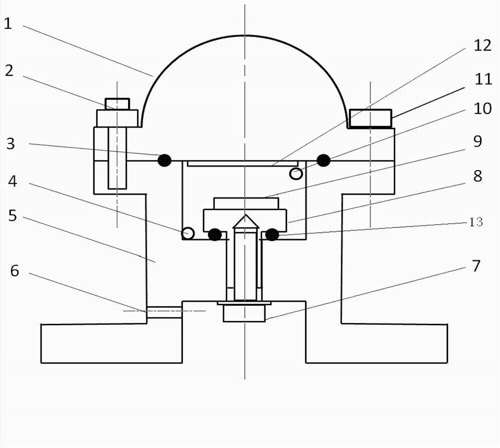
Electrochemical-optical combined in-situ study spectral cell
An electrochemical and spectral cell technology, applied in the field of spectral cells, can solve the problems of reducing the absorption of spectral signals by the solution, failing to reflect the formation process and dynamic evolution mechanism of the SEI film, and unable to accurately reflect the in-situ state of the SEI film, etc., to achieve an effective principle Spectral characterization, avoiding the effect of absorption
- Summary
- Abstract
- Description
- Claims
- Application Information
AI Technical Summary
Problems solved by technology
Method used
Image
Examples
Embodiment 1
[0027] like figure 1 As shown, a lithium sheet is used as the reference electrode 9 and the counter electrode, fixed on the sample stage 8 by conductive glue, and SiO 2 The crystal is used as the current collector of the working electrode and the semi-cylindrical crystal light-transmitting window 1, in SiO 2 A layer of active material SnS is coated on the surface of the bottom plane of the semi-cylindrical crystal light-transmitting window 1 of the crystal 2 thin film (thickness 100 nm) as the working electrode 12, and the active material SnS 2 The film layer is covered on the cell body 5 downwards, and then fixed. Working electrode 12 (i.e. active material SnS 2 The thin film layer) is connected with a wire through conductive glue, and the reference electrode 9 is connected with a wire through the fastening bolt 7 of the sample stage, and both electrodes are connected with the electrochemical workstation through wires. Adjust the optical path so that the incident light of...
Embodiment 2
[0029] Adopt lithium sheet as reference electrode 9 and counter electrode, be fixed on the sample stage 8 by conductive glue, adopt Al 2 o 3 The crystal is used as the current collector of the working electrode and the semi-cylindrical crystal light-transmitting window 1, in Al 2 o 3 The bottom plane surface of the semi-cylindrical crystal light-transmitting window 1 of the crystal is coated with a layer of active material ZnS thin film (thickness is 50 nanometers) as the working electrode 12, and the active material ZnS thin film layer is covered on the pool body 5 downwards , then fixed. The working electrode 12 (that is, the active material ZnS thin film layer) is connected with a wire through conductive glue, and the reference electrode 9 is connected with a wire through the fastening bolt 7 of the sample stage, and both electrodes are connected with the electrochemical workstation through wires. Adjust the light path, after reflection, make the incident light of the sp...
Embodiment 3
[0031] A lithium sheet is used as the reference electrode 9 and the counter electrode, fixed on the sample stage 8 by conductive glue, and CaF 2 The crystal is used as the current collector of the working electrode and the semi-cylindrical crystal light-transmitting window 1, in CaF 2 The bottom plane surface of the semi-cylindrical crystal light-transmitting window 1 of the crystal is coated with a layer of active material Si film (thickness is 80 nanometers) as the working electrode 12, and the active material Si film layer is covered on the cell body 5 downwards, and then fixed. The working electrode 12 (that is, the active material Si film layer) is connected with a wire through the conductive glue, and the reference electrode 9 is connected with the wire through the fastening bolt 7 of the sample stage, and both electrodes are connected with the electrochemical workstation through the wire. Adjust the optical path so that the incident light of the spectrometer hits the s...
PUM
| Property | Measurement | Unit |
|---|---|---|
| Thickness | aaaaa | aaaaa |
Abstract
Description
Claims
Application Information
 - R&D Engineer
- R&D Manager
- IP Professional
- Industry Leading Data Capabilities
- Powerful AI technology
- Patent DNA Extraction
Browse by: Latest US Patents, China's latest patents, Technical Efficacy Thesaurus, Application Domain, Technology Topic, Popular Technical Reports.
© 2024 PatSnap. All rights reserved.Legal|Privacy policy|Modern Slavery Act Transparency Statement|Sitemap|About US| Contact US: help@patsnap.com


