Chip LED and manufacturing method thereof

A CHIP-LED and manufacturing method technology, applied in electrical components, electrical solid devices, circuits, etc., can solve the problems of conductive vias overflowing glue, affecting product quality, etc., to reduce surface tension, improve welding performance, and improve quality. Effect

Active Publication Date: 2015-04-01
HONGLI ZHIHUI GRP CO LTD
View PDF5 Cites 0 Cited by
  • Summary
  • Abstract
  • Description
  • Claims
  • Application Information

AI Technical Summary

Problems solved by technology

When using the above process to make CHIP-LED, due to the formation of conductive vias on the substrate, when the optical lens is molded, there will be glue overflow at the conductive vias, which will affect product quality.

Method used


Image

  • Chip LED and manufacturing method thereof

Examples


Embodiment Construction

[0017] The present invention will be further described in detail below in conjunction with the accompanying drawings and specific embodiments.

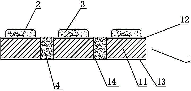
[0018] Such as figure 1 As shown, the CHIP-LED includes a substrate 1 and an LED chip 2. The substrate 1 includes a body 11, a front circuit layer 12 arranged on the upper surface of the body, a back circuit layer 13 arranged on the lower surface of the body, and a circuit layer 13 arranged on the body. The conductive via hole 14 on the top and the connection circuit layer arranged on the inner wall of the conductive via hole for electrically connecting the front circuit layer and the back circuit layer; the LED chip 2 is installed on the front circuit layer through the solid crystal bonding process; The via holes are filled with rosin 5 .

[0019] The method of manufacturing the above-mentioned CHIP-LED is as follows.

[0020] (1) Fabricate the substrate 1 .

[0021] (2) Install a backing plate on the lower surface of the substrat...


PUM


Abstract

The invention discloses a chip LED and a manufacturing method thereof. The chip LED comprises a substrate and an LED chip. The substrate comprises a body, a front circuit layer on the upper surface of the body, a back circuit layer on the lower surface of the body, conducing vias on the body, and connecting circuit layers, wherein the connecting circuit layers used for electrically connecting the front circuit layer and the back circuit layer are arranged in the conducting vias. The LED chip is mounted on the front circuit layer by die bonding and wire bonding. The conducting vias are filled with rosin. The manufacturing method includes the sequential steps of substrate manufacturing, rosin filling, die bonding and wire bonding, baking, and cutting. By the use of the chip LED and the manufacturing method thereof, excessive glue can be avoided in compression molding process and product quality can be improved.

Description

technical field [0001] The invention relates to an LED and a manufacturing method thereof. Background technique [0002] The existing CHIP-LED is mainly composed of a substrate, an LED chip and an optical lens, wherein the substrate includes a body, a front circuit layer arranged on the upper surface of the body, a back circuit layer arranged on the lower surface of the body, and a conductive circuit layer arranged on the body. The via hole and the connection circuit layer on the inner wall of the conductive via that electrically connect the front circuit layer and the back circuit layer, the LED chip is installed on the front circuit layer, and the LED chip is realized through the process of solid crystal bonding. The electrical connection of the front circuit layer and the optical mirror are realized through the compression molding process. When making CHIP-LEDs by using the above-mentioned process, due to the formation of conductive via holes on the substrate, when ...

Claims


Application Information

Patent Timeline
Patent Type & Authority Patents(China)
IPC IPC(8): H01L33/48H01L33/62
CPCH01L2224/48091H01L2924/181
Inventor 钟金文殷小平王高阳王跃飞周小泉李国平
Owner HONGLI ZHIHUI GRP CO LTD
Why Eureka
Try Eureka