
A method of producing directionally solidified polycrystalline silicon ingots

A polycrystalline silicon ingot, directional solidification technology, applied in polycrystalline material growth, chemical instruments and methods, crystal growth, etc., can solve the problems of increasing the temperature and time of silicon ingots, reduce dislocation density, shorten production cycle, and reduce production Effect of Energy Consumption and Argon Consumption

Active Publication Date: 2016-01-27
NANCHANG UNIV
View PDF7 Cites 0 Cited by
  • Summary
  • Abstract
  • Description
  • Claims
  • Application Information

AI Technical Summary

Problems solved by technology

In addition, such a process brings additional man-hours, power consumption and argon gas consumption, and also increases the temperature and time at which the silicon ingot, especially its bottom, is contaminated by the thermal diffusion of the crucible

Method used


Image

  • A method of producing directionally solidified polycrystalline silicon ingots
  • A method of producing directionally solidified polycrystalline silicon ingots
  • A method of producing directionally solidified polycrystalline silicon ingots

Examples


Embodiment 1

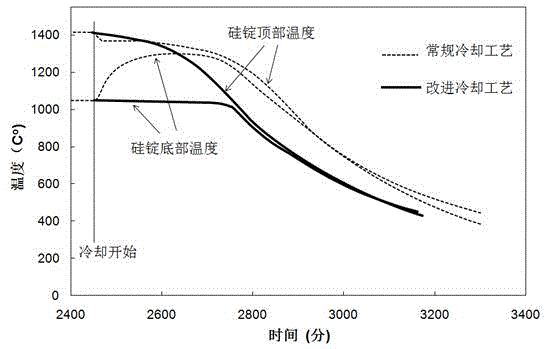
[0016] Polysilicon ingots are grown in a 450-kilogram directional solidification polysilicon furnace with an ordinary lifting and insulating cage type (such as produced by GT in the United States). The material of the crucible is high-purity quartz ceramics, the size is 840x840x350mm 3 . After the silicon ingot completes solidification and growth in the furnace, it enters the cooling stage. By adjusting and controlling the power of the furnace heater and the width of the heat dissipation channel below the bottom of the crucible, two cooling processes, conventional cooling and the improved cooling of the present invention, are realized respectively, and the conventional cooling polysilicon ingot and the improved cooling polysilicon ingot are obtained, and the cooling time of the latter is shortened by about 2 times compared with the former Hour.

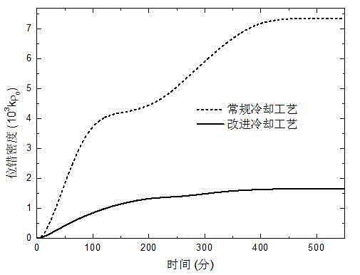
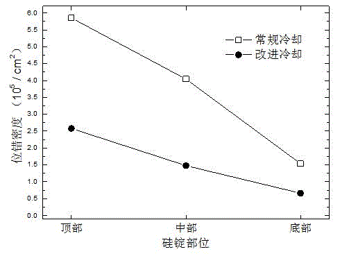
[0017] After the two kinds of silicon ingots were sectioned, samples were sampled and polished at different parts and dislocations...

Embodiment 2

[0023] Polysilicon ingots are grown in a 450-kilogram directional solidification polysilicon furnace using an ordinary lifting and insulating base type (such as that produced by China Jinggong). The material of the crucible is high-purity quartz ceramics, the size is 840x840x350mm 3 . After the silicon ingot completes solidification and growth in the furnace, it enters the cooling stage. By adjusting and controlling the power of the furnace heater and the width of the heat dissipation channel below the bottom of the crucible, two cooling processes, conventional cooling and improved cooling, are realized respectively, and conventional cooling polysilicon ingots and improved cooling polysilicon ingots are obtained. The cooling time of the latter is about 2.5 hours shorter than that of the former.

[0024] After the two silicon ingots were cut, samples were polished at different parts and dislocations were etched. After that, the etched surface was randomly sampled under the con...


PUM

PropertyMeasurementUnit
sizeaaaaaaaaaa

Abstract

A method for producing a directional solidified polycrystalline silicon ingot comprises the steps of heating for melting, crystal growth solidification and cooling, and is characterized in that in the stage of cooling, the opening of heat dissipation passages at the bottom of the polycrystalline silicon ingot is kept so as to enable the bottom temperature of the polycrystalline silicon ingot to be continuously and slowly descended following the former trend; and at the same time, heating power of a stove is gradually reduced to enable the temperature of the polycrystalline silicon ingot to be continuously descended, and the polycrystalline silicon ingot can be taken out of the stove until the temperature of the polycrystalline silicon ingot is below 300 DEG C. The method greatly reduces dislocation density of the directional solidified polycrystalline silicon ingot, shortens the producing cycle of the directional solidified polycrystalline silicon ingot, reduces production energy consumption and argon consumption, and reduces diffusion pollution of a crucible on a silicon ingot.

Description

technical field [0001] The invention belongs to the technical field of polycrystalline silicon ingot production. In particular, it relates to a method for producing directionally solidified polycrystalline silicon ingots for solar cells. Background technique [0002] More than 85% of the modern photovoltaic industry is based on crystalline silicon wafer solar cells, more than half of which are made of directional solidified polysilicon materials. This kind of material generally has the problems of high internal dislocation defect density and the problem that the bottom and side of the ingot are polluted by the thermal diffusion of metal impurities in the crucible. Both dislocations and metal impurities can seriously impair the performance of silicon crystals for photovoltaic applications. [0003] So far, in the production process of this kind of polycrystalline silicon ingot, such a cooling process is generally used in the cooling stage after solidification: first, the te...

Claims


Application Information

Patent Timeline
Patent Type & Authority Patents(China)
IPC IPC(8): C30B28/06C30B29/06
Inventor 周浪周耐根林茂华
Owner NANCHANG UNIV
Learn More