
Additional-voltage-free zero voltage switch bridge-free power factor corrector and modulation method

A technology of power factor correction and zero-voltage switching, which is applied in the direction of high-efficiency power electronic conversion, output power conversion devices, electrical components, etc., can solve the problems of lower circuit efficiency, large device switching loss, and large electromagnetic interference, etc., to improve the circuit Efficiency, increase power density, increase the effect of operating frequency

Active Publication Date: 2013-03-13
SHANGHAI JIAODA INTELLECTUAL PORPERTY MANAGEMENT CO LTD +1
View PDF7 Cites 8 Cited by
  • Summary
  • Abstract
  • Description
  • Claims
  • Application Information

AI Technical Summary

Problems solved by technology

However, the circuit works in a hard switching state, there is a problem of reverse recovery of the diode, and the switching loss of the device is large, which limits the improvement of the operating frequency, reduces the circuit efficiency and has a large electromagnetic interference

Method used


Image

  • Additional-voltage-free zero voltage switch bridge-free power factor corrector and modulation method
  • Additional-voltage-free zero voltage switch bridge-free power factor corrector and modulation method
  • Additional-voltage-free zero voltage switch bridge-free power factor corrector and modulation method

Examples


Embodiment Construction

[0023] The present invention will be described in detail below in conjunction with specific embodiments. The following examples will help those skilled in the art to further understand the present invention, but do not limit the present invention in any form. It should be noted that those skilled in the art can make several modifications and improvements without departing from the concept of the present invention. These all belong to the protection scope of the present invention.

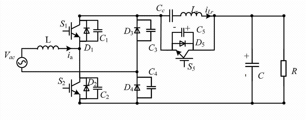
[0024] refer to image 3 , the present invention has no additional voltage zero-voltage switch bridgeless power factor corrector, including DC side load R, DC side capacitor C, composed of two antiparallel diodes D 1 ~D 2 The fully controlled main switch S 1 ~S 2 A bridge arm consisting of two diodes D 3 ~D 4 Constitute another bridge arm, connected to the input filter inductance L between the midpoint of the bridge arm and the AC grid, where: two main switches S 1 ~S 2 Parallel capacitor C...


PUM


Abstract

The invention provides an additional-voltage-free zero voltage switch bridge-free power factor corrector and a modulation method. The corrector comprises a power factor corrector direct current side load, a direct current side capacitor, an alternating current filtering capacitor, a bridge arm formed by two full control main switches with antiparallel diodes and a bridge arm formed by connecting two diodes in series. An antiparallel diode auxiliary switch is connected between bridge arm side direct current buses formed by directly connecting the direct current side capacitor and the diodes. Capacitors are arranged at two ends of the main switches and the auxiliary switch in parallel, capacitors are connected at two ends of the diodes on the bridge arm in parallel, and resonant branches formed by connecting resonant inductors and clamping capacitors are in bridge joint with two ends of the auxiliary switch. The main switches adopt the sine wave pulse width modulation method, and demodulation signals of the auxiliary switch are synchronous with those of the main switches. The corrector is simple in structure, and the direct current output can serve as a direct current power supply in use. The corrector is small in switch consumption, high in circuit efficiency and favorable for improving working efficiency and further improves power accuracy.

Description

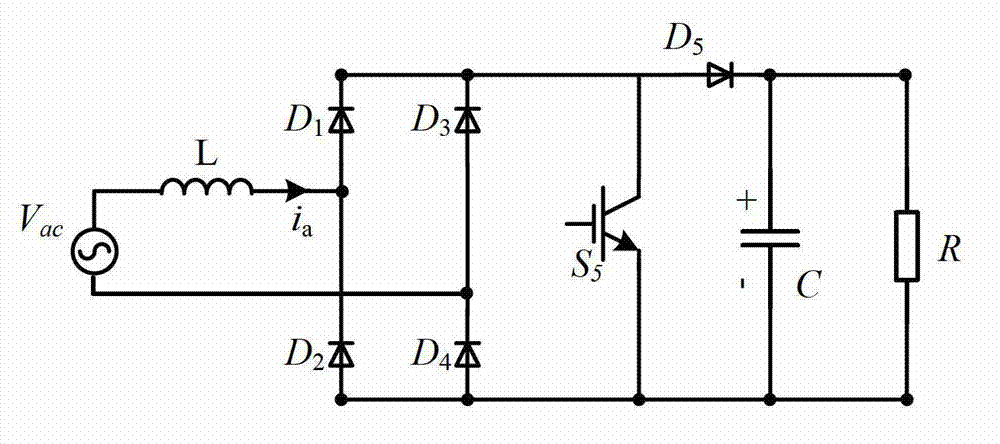
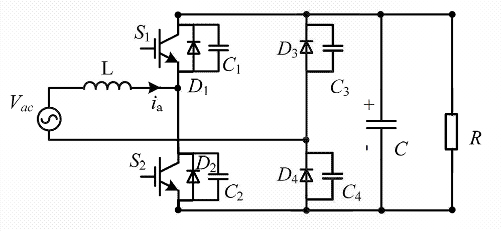
technical field [0001] The invention relates to a bridgeless power factor corrector, in particular to a circuit topology and modulation method of a bridgeless power factor corrector with no additional voltage stress and a zero-voltage switch bridgeless power factor corrector. Background technique [0002] The current general single-phase power factor corrector, its circuit is as follows figure 1 shown, it consists of four diodes D 1 ~D 4 The bridge arm of the single-phase full bridge is connected to the input filter inductance L between the midpoint of the bridge arm and the AC power grid. This single-phase power factor corrector can be used as a communication power supply, etc., but there are many diodes in the loop channel of this circuit, and the conduction loss is relatively large. In order to reduce the conduction loss of the diode, a bridgeless power factor corrector is proposed, and its circuit is as follows figure 2 As shown, it consists of two fully controlled ...

Claims


Application Information

Patent Timeline
Patent Type & Authority Applications(China)
IPC IPC(8): H02M1/42
CPCY02B70/126Y02B70/1491Y02B70/10Y02P80/10
Inventor 李睿王艺翰梁星蔡旭
Owner SHANGHAI JIAODA INTELLECTUAL PORPERTY MANAGEMENT CO LTD
Learn More