
GaN heterojunction HEMT (High Electron Mobility Transistor) device

A heterojunction and device technology, applied in semiconductor devices, electrical components, circuits, etc., can solve the problems of increasing the off-state breakdown voltage of the device, increasing the cost of the device, pushing up the wafer area, etc., and achieving off-state breakdown. The effect of higher voltage, smaller wafer area, and lower device cost

Inactive Publication Date: 2013-02-27
UNIV OF ELECTRONICS SCI & TECH OF CHINA
View PDF4 Cites 16 Cited by
  • Summary
  • Abstract
  • Description
  • Claims
  • Application Information

AI Technical Summary

Problems solved by technology

This solution is at the cost of sacrificing the on-resistance of the device, and it also increases the wafer area required for a single device, which eventually leads to an increase in the cost of the device, which does not conform to the theory of seeking the optimal value of the on-resistance and breakdown voltage of the device.
On the other hand, the field plate structure can effectively increase the off-state breakdown voltage of the device, but the process steps are more complicated than devices without field plates, and the effect of the field plate structure is closely related to the quality of the dielectric layer material
Therefore, it is a more complicated problem to improve the off-state breakdown voltage of the device through the field plate structure.

Method used


Image

  • GaN heterojunction HEMT (High Electron Mobility Transistor) device
  • GaN heterojunction HEMT (High Electron Mobility Transistor) device
  • GaN heterojunction HEMT (High Electron Mobility Transistor) device

Examples


Embodiment Construction

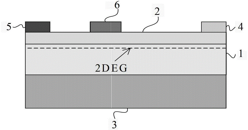
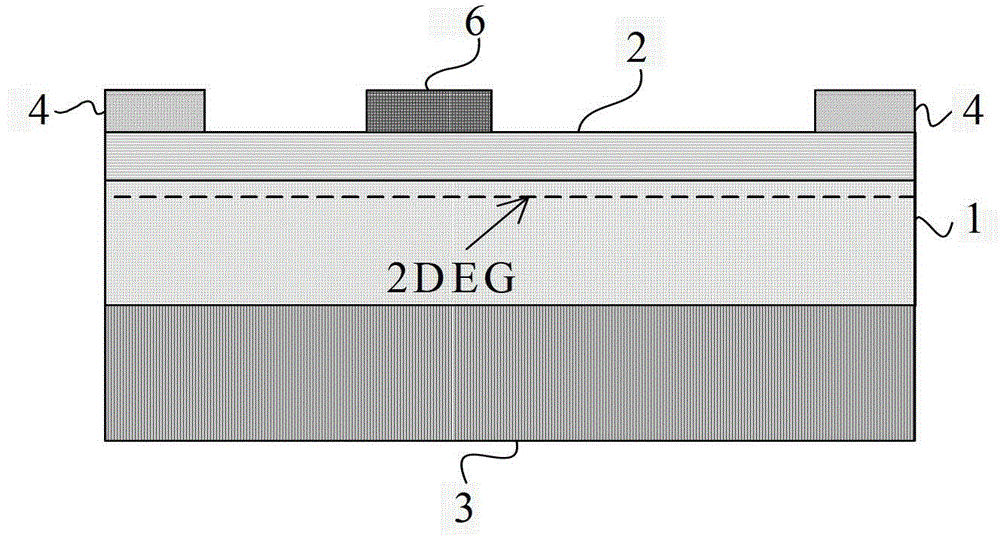
[0022] The Schottky source high-voltage InAlN / GaN HEMTs device provided by the present invention (such as figure 1 shown), including a substrate 3, a GaN layer 1 on the surface of the substrate 3, and an InAlN layer 2 on the surface of the GaN layer 1; where the GaN layer 1 and the InAlN layer 2 form an InAlN / GaN heterojunction, and the InAlN / GaN heterojunction A two-dimensional electron gas (2DEG) conductive channel is formed at the junction interface; there are gate electrodes 6, source electrodes 5 and drain electrodes 4 on the surface of the InAlN layer 2, wherein the source electrodes 5 and drain electrodes 4 are located on the opposite sides of the InAlN layer 2 surface The gate electrode 6 is located between the source electrode 5 and the drain electrode 4; the drain electrode 4 forms an ohmic contact with the surface of the InAlN layer 2, and the source electrode 5 forms a Schottky contact with the surface of the InAlN layer 2.

[0023] The GaN heterojunction HEMT devi...


PUM


Abstract

The invention discloses a GaN heterojunction HEMT (High Electron Mobility Transistor) device, belonging to the technical field of semiconductor devices. The GaN heterojunction HEMT device comprises a substrate and an InAIN / GaN heterojunction, wherein the InAIN / GaN heterojunction is positioned on the surface of the substrate; the surface of an InAIN layer is provided with a grid electrode, a source electrode and a drain electrode; and the drain electrode and the surface of the InAIN layer form ohmic contact, while the source electrode and the surface of the InAIN layer form Schottky contact. The GaN heterojunction HEMT device disclosed by the invention has the advantages that the Schottky contact is adopted at the source electrode, the electric field in GaN under the source electrode is uniformly distributed due to a good appearance characteristic, the electron injection of the source electrode is effectively restrained, and the current leakage of GaN and collision ionization and current leakage of the grid electrode caused by the current leakage are reduced, so that the off-state puncture voltage of the device is improved; the drain electrode adopts ohmic contact still, so that the positive on resistance of the device is reduced as low as possible, and better positive current driving capability of the device is ensured; in addition, the GaN heterojunction HEMT device is compatible to the traditional process, simultaneously the distance between the grid electrode and the source electrode can be very short, and the wafer occupying area is smaller, so that lower cost of the device is ensured.

Description

technical field [0001] The invention belongs to the technical field of semiconductor devices and relates to a GaN heterojunction electron mobility transistor (HEMT). Background technique [0002] Gallium nitride (GaN) is one of the representatives of the third-generation wide-bandgap semiconductor materials, with excellent characteristics: high critical breakdown electric field (~3.3×10 6 V / cm), high electron mobility (~2000cm 2 / V·s), high two-dimensional electron gas (2DEG) concentration (~10 13 cm -2 ), good high temperature working ability. High electron mobility transistors (HEMTs) based on GaN materials have been applied in the semiconductor field, especially in the radio frequency / microwave field, and have been used in wireless communication, satellite communication, etc. In addition, for power electronics applications, this type of device has the characteristics of high reverse blocking voltage, low forward conduction resistance, and high operating frequency, so ...

Claims


Application Information

Patent Timeline
Patent Type & Authority Applications(China)
IPC IPC(8): H01L29/778
Inventor 周琦陈万军尉中杰张波
Owner UNIV OF ELECTRONICS SCI & TECH OF CHINA
Learn More