Inductor structure

A technology of inductance and on-chip inductance, applied in circuits, electrical components, electrical solid devices, etc., can solve the problem of not effectively utilizing the area of ​​the inductance, and achieve the effect of saving the occupied area.

Active Publication Date: 2013-02-20
SHANGHAI INTEGRATED CIRCUIT RES & DEV CENT
View PDF4 Cites 8 Cited by
  • Summary
  • Abstract
  • Description
  • Claims
  • Application Information

AI Technical Summary

Problems solved by technology

It is worth noting that since the area of ​​the inductor is usually large (such as 300 microns × 300 microns), making a passive shielding layer below it can certainly play the role of electromagnetic isolation, but it does not effectively use the area under the inductor

Method used


Image

  • Inductor structure
  • Inductor structure
  • Inductor structure

Examples


Embodiment Construction

[0018] In order to make the content of the present invention clearer and easier to understand, the content of the present invention will be further described below in conjunction with the accompanying drawings. Of course, the present invention is not limited to this specific embodiment, and general replacements known to those skilled in the art are also covered within the protection scope of the present invention.

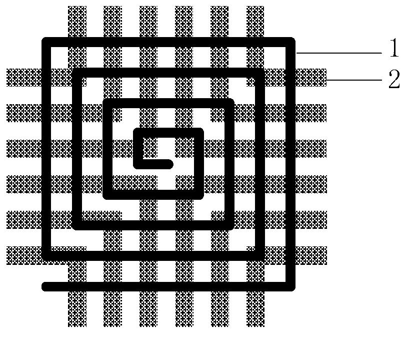
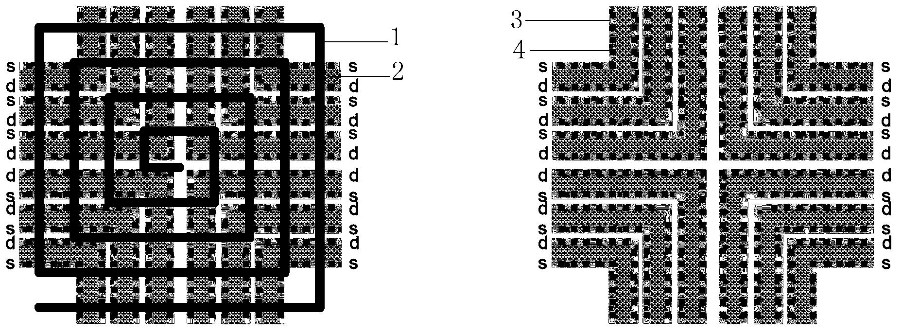
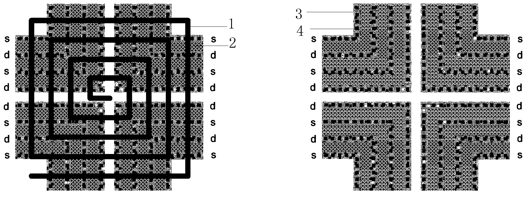
[0019] The inductance structure of the present invention includes an on-chip inductor and a shielding layer located under the on-chip inductor. Wherein, the on-chip inductor is made of a top layer metal and a second top layer metal, and the shielding layer includes a plurality of shielding units, and these shielding units form at least one shielding area. The arrangement of these shielding units is the same as the arrangement of the first layer of metal in the passive shielding isolation layer in the prior art, that is, it is perpendicular to the direction of the e...


PUM


Abstract

The invention discloses an inductor structure which comprises an on-chip inductor and a shielding layer positioned below the on-chip inductor, wherein the shielding layer comprises multiple shielding units; the shielding units are orthogonal to the direction of eddy current generated by the on-chip inductor; the shielding units are composed of MOS (metal oxide semiconductor) transistors or metal wires or polysilicon; at least one among the shielding units is composed of MOS transistors; and source electrodes and drain electrodes of the MOS transistors are grounded. According to the inductor structure, the area below the on-chip inductor is fully utilized to realize the function of a voltage stabilizing transistor.

Description

technical field [0001] The invention relates to the field of integrated circuits, in particular to an inductance structure on an integrated circuit chip. Background technique [0002] Inductors are important passive components in the front-end of RF transceivers. The RF front-end transceiver modules that need to use integrated inductors mainly include: inductor structure, power amplifier, oscillator, up-conversion mixer, etc. Inductors play an important role in these modules. [0003] Taking the inductance structure as an example, the inductance structure is one of the important modules in the radio frequency transceiver. It is mainly used in the communication system to amplify the signal received from the antenna, which is convenient for the subsequent receiver circuit processing. It is precisely because the noise amplifier is located at the first stage of the entire receiver close to the antenna, its characteristics directly affect the quality of the signal received by th...

Claims


Application Information

Patent Timeline
Patent Type & Authority Applications(China)
IPC IPC(8): H01L23/64
CPCH01L2924/0002
Inventor 李琛皮常明温建新
Owner SHANGHAI INTEGRATED CIRCUIT RES & DEV CENT
Why Eureka
Try Eureka