Packaging structure without external pin

A technology of packaging structure and external pins, which is applied in the direction of semiconductor/solid-state device components, semiconductor devices, electrical components, etc., can solve the problems of excessively long hanging parts of pins, increased cost, shaking and deformation, and avoid electrical performance The effect of reducing, shortening length and reducing production cost

Active Publication Date: 2013-02-13
CHIPMOS TECH INC
View PDF2 Cites 1 Cited by
  • Summary
  • Abstract
  • Description
  • Claims
  • Application Information

AI Technical Summary

Problems solved by technology

Furthermore, changing the design of the chip holder and pins may cause the suspension part of the pins to be too long and cause fear of shaking and deformation, or the external components (such as printed circuit boards) in the subsequent process must also be changed accordingly, resulting in cost. Increase

Method used


Image

  • Packaging structure without external pin
  • Packaging structure without external pin
  • Packaging structure without external pin

Examples


Embodiment Construction

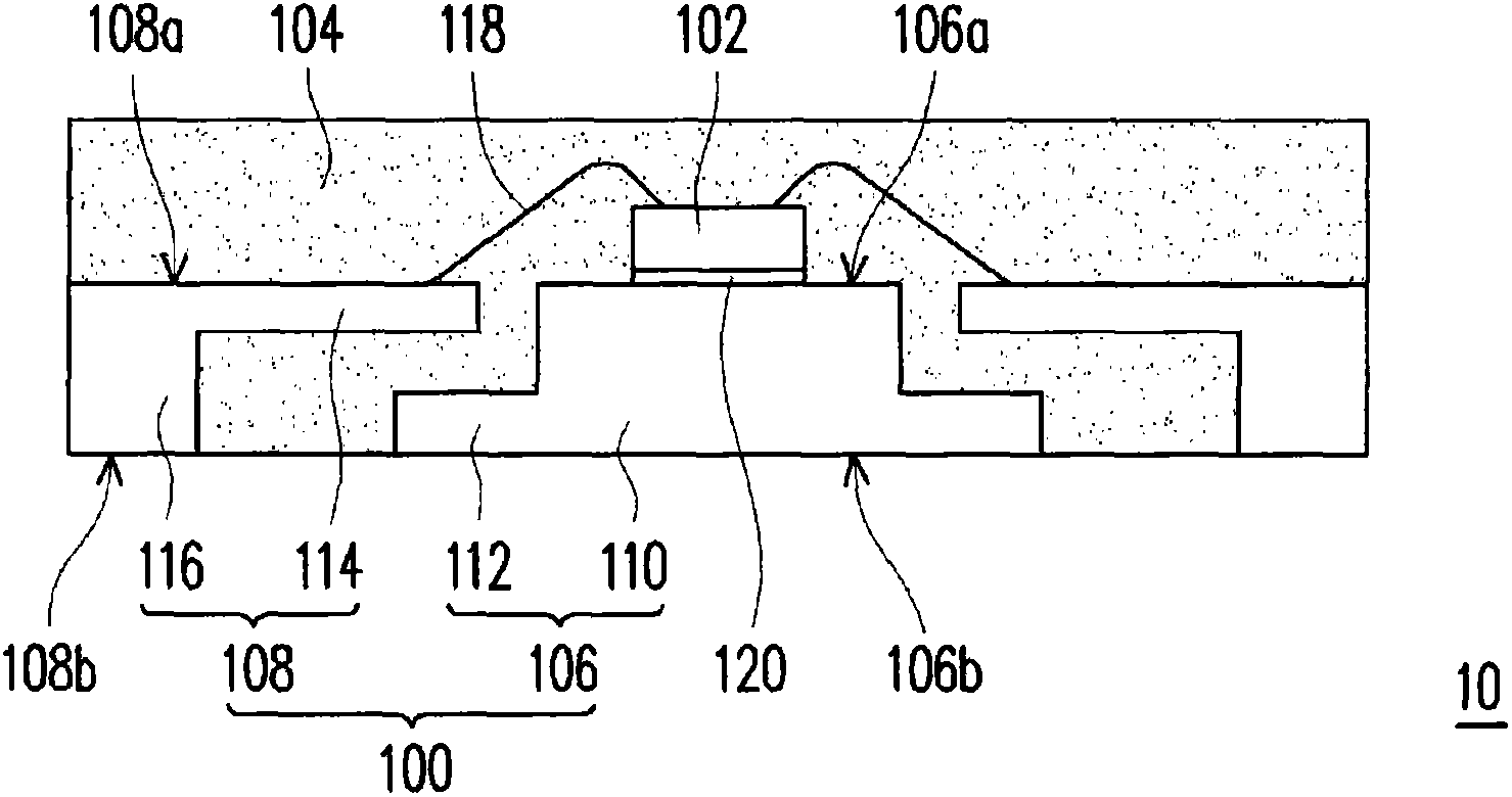
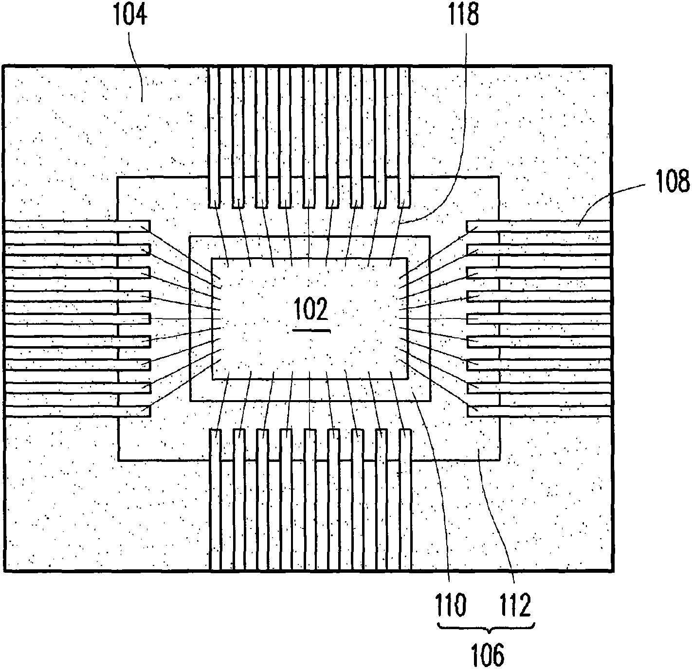
[0018] figure 1 It is a schematic cross-sectional view of a leadless package structure according to an embodiment of the present invention. figure 2 for figure 1 The schematic diagram of the top view of the package structure without external pins. exist figure 2 In , the number of pins is only for illustration, and is not intended to limit the present invention. Please refer to figure 1 and figure 2 , the leadless package structure 10 of this embodiment includes a lead frame 100 , a chip 102 and an encapsulant 104 . The lead frame 100 includes a die paddle 106 and a plurality of pins 108 . The die paddle 106 has a top surface 106a and a bottom surface 106b. In addition, the die holder 106 includes a die bonding portion 110 and a peripheral portion 112 . The peripheral portion 112 connects to and surrounds the die bonding portion 110 . The chip bonding portion 110 is used for disposing the chip 102 thereon.

[0019] In this embodiment, the top surface 106 a of the ...


PUM


Abstract

A packaging structure without external pins comprises a wire rack, a chip, and a packaging colloid. The wire rack comprises a chip seat and a plurality of pins. The pin seat has a top surface and a bottom surface, and the chip seat comprises a chip jointing portion and a periphery portion. The periphery portion connects and encircles the chip jointing portion. The top surface of the chip seat outside the chip jointing portion is depressed to form the periphery portion. The pins are configured around the chip seat and are electrically separated from the chip seat. Each pin has a top surface and a bottom surface, and each pin comprises a cantilever portion and an external connection portion. Bottom surface of the pins outside the external connection portion are depressed to form the cantilever portions. The cantilever portion extends above the periphery portion from the external connection portion and partially overlaps with the periphery portion. The chip is configured on the chip jointing portion and electrically connected to the cantilever portion through a plurality of bonding wires. And the packaging colloid covers the chip, the bonding wires, and the wire rack.

Description

technical field [0001] The present invention relates to a chip packaging structure, and in particular to a packaging structure without external leads. Background technique [0002] Semiconductor packaging technology includes many packaging forms. With the trend of miniaturization and thinning of chip packaging structures, a quad flat no-lead (QFN) package belonging to the flat package series has been developed. The QFLN package can be greatly reduced in size because there are no outwardly extending pins, and it has a shorter signal transmission path and a relatively faster signal transmission speed. Therefore, the quad flat no-lead package is very suitable for high-speed and high-frequency products with medium and low pin counts, and has become one of the mainstreams of this type of package. [0003] In the QFN package structure, there is a gap between the die pad and the lead to electrically separate the two. In addition, the chip is mounted on the chip holder and is elec...

Claims


Application Information

Patent Timeline
Patent Type & Authority Applications(China)
IPC IPC(8): H01L23/31H01L23/495H01L23/367
CPCH01L24/73H01L2224/32245H01L2224/48247H01L2224/73265H01L2924/181H01L2924/00012
Inventor 杜武昌刘立中刘志益
Owner CHIPMOS TECH INC
Why Eureka
Try Eureka