Resistance random access memory based on vanadium oxide/zinc oxide laminated structure and preparation method thereof
A technology of resistive memory and stacked structure, which is applied in the field of microelectronics to achieve the effect of improving consistency and repeatability
- Summary
- Abstract
- Description
- Claims
- Application Information
AI Technical Summary
Problems solved by technology
Method used
Image
Examples
Embodiment 1
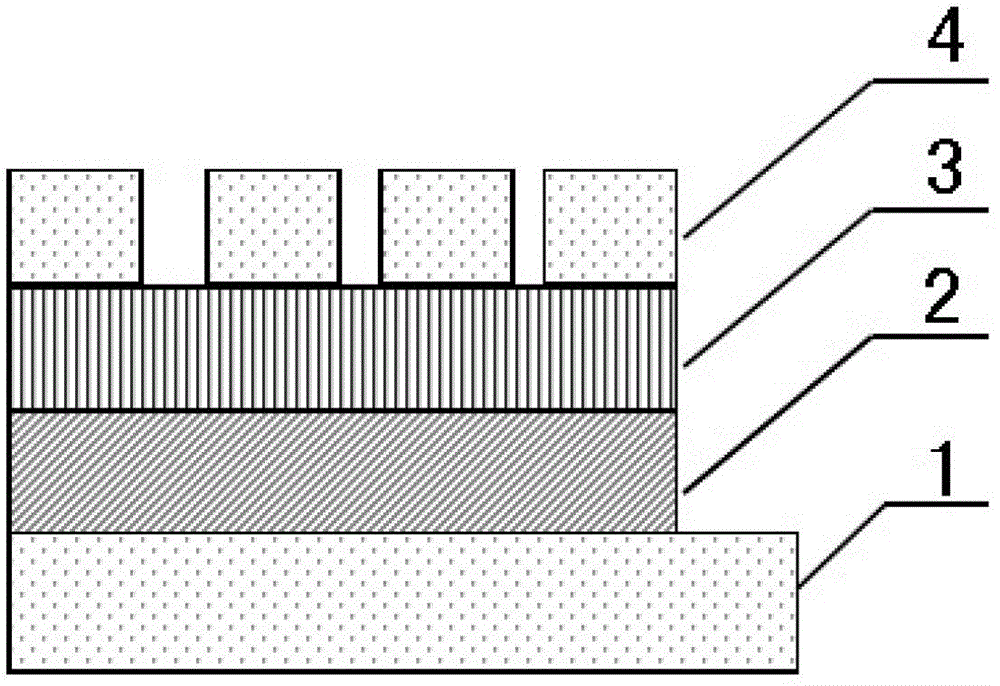
[0029] A resistive variable memory based on a vanadium oxide / zinc oxide stack structure, such as figure 1 As shown, it is composed of a lower electrode 1, a resistive layer and an upper electrode 4. The resistive layer is a laminated structure composed of a vanadium oxide dielectric layer 2 and a zinc oxide dielectric layer 3. The composition of zinc oxide is ZnO 1-x , where x is 0.1, the thickness of the zinc oxide dielectric layer is 30nm; the composition of vanadium oxide is VO y , wherein y is 0.15, the thickness of the vanadium oxide dielectric layer is 30nm; the lower electrode is Pt, the thickness is 50nm, and the upper electrode is W, the thickness is 50nm.
[0030] The preparation method of the resistive memory, the steps are as follows:
[0031] 1) Si wafers are used as substrates, and SiO is prepared on silicon substrates by thermal oxidation using an oxidation diffusion furnace. 2 Insulation;
[0032] 2) On SiO 2 A 10nm thick Ti adhesion layer was prepared on t...
Embodiment 2
[0040]A resistive variable memory based on a vanadium oxide / zinc oxide laminated structure, the structure is basically the same as that of Embodiment 1, except that W is the lower electrode with a thickness of 50nm, and TiN is the upper electrode with a thickness of 100nm.
[0041] The preparation method of the resistive memory, the steps are as follows:
[0042] 1), 2) are the same as embodiment 1;
[0043] 3) On the Ti adhesion layer, deposit a tungsten lower electrode with a thickness of 50nm by DC magnetron sputtering. The process parameters of DC magnetron sputtering: the target is a φ60mm metal tungsten target, the target intercept is 6.5cm, and the working pressure is 0.5 Pa, Ar flow rate is 20sccm, sputtering power is 50W;
[0044] 4) Deposit a vanadium oxide film with a thickness of 30nm on the lower electrode by radio frequency sputtering. The sputtering process conditions are: the target is a φ60mm vanadium oxide ceramic target, the target intercept is 6.5cm, and t...
Embodiment 3
[0050] A resistive variable memory based on a vanadium oxide / zinc oxide stack structure, the structure is basically the same as that of embodiment 1, the difference is that W is the bottom electrode, W is the top electrode, and the thickness is 50nm.
[0051] The preparation method of the RRAM, the steps and the preparation process of the W electrode are the same as those in Example 1.
PUM
| Property | Measurement | Unit |
|---|---|---|
| thickness | aaaaa | aaaaa |
| thickness | aaaaa | aaaaa |
| thickness | aaaaa | aaaaa |
Abstract
Description
Claims
Application Information
 - R&D
- Intellectual Property
- Life Sciences
- Materials
- Tech Scout
- Unparalleled Data Quality
- Higher Quality Content
- 60% Fewer Hallucinations
Browse by: Latest US Patents, China's latest patents, Technical Efficacy Thesaurus, Application Domain, Technology Topic, Popular Technical Reports.
© 2025 PatSnap. All rights reserved.Legal|Privacy policy|Modern Slavery Act Transparency Statement|Sitemap|About US| Contact US: help@patsnap.com


