Pretreatment method for silylation and silylation method comprising same

A monosilane and pretreatment technology, which is applied in the manufacture of electrical components, semiconductor/solid-state devices, circuits, etc., can solve problems such as peeling, particles in the layer, and failure of resist patterns, and achieve the effect of improving product yield

Active Publication Date: 2016-02-17
SEMICON MFG INT (SHANGHAI) CORP
View PDF3 Cites 0 Cited by
  • Summary
  • Abstract
  • Description
  • Claims
  • Application Information

AI Technical Summary

Problems solved by technology

[0004] However, if the silylation agent does not react uniformly with the wafer surface, or if there are particles, water, or chemical residues in the processing chamber or wafer surface, the product will have defects such as peeling, particles in the layer, or bubbles, etc., resulting in corrosion resistance. pattern failed

Method used


Image

  • Pretreatment method for silylation and silylation method comprising same

Examples


Embodiment 1

[0027] The system for silylation includes: a heating system, a processing chamber, a silylating agent input port, a nitrogen gas input port, an exhaust port, a vacuum system, and a control module.

[0028] Turn on the heating system, control the constant temperature of the processing chamber at 125°C, put the wafer to be processed into the processing chamber, blow in nitrogen, and control the flow rate to 10,000 milliliters / minute (ml / min). After 10s, the mixed gas of HMDS and nitrogen is introduced. The volume ratio of HMDS and nitrogen is: 45:55. After the control flow is 15s, the mixed gas is stopped and the nitrogen is continued. The control flow is 2000 ml / min (ml / min ), and exhaust from the exhaust port.

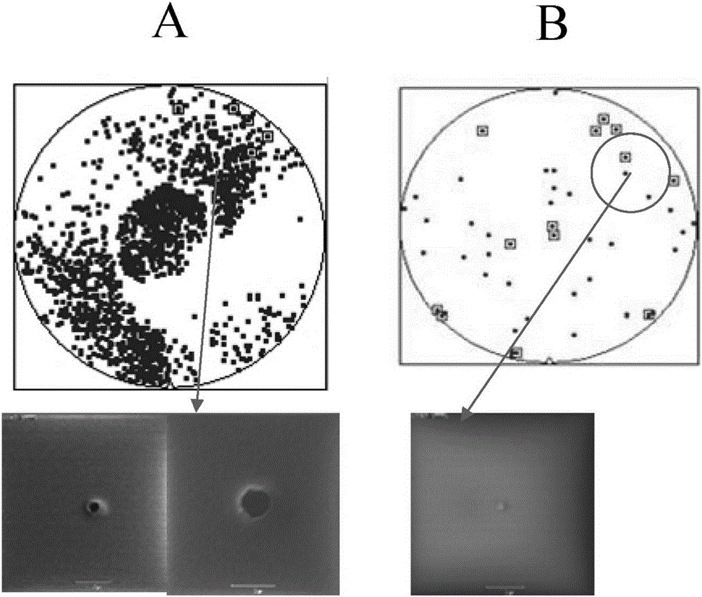
[0029] The whole process is controlled by the control module, and the processing chamber temperature is kept constant during the process. After the pretreatment, the wafers were subjected to a general silylation treatment, and the obtained wafers were subjected to a c...


PUM


Abstract

The invention relates to a pretreatment method for silanization, which is characterized in before performing silanization to a wafer, performing the following steps: heating the wafer, and introducing nitrogen to purge; introducing diluted silanization agent gas; and introducing the nitrogen to purge continuously, and exhausting the gas. The invention further relates to a silanization method comprising the pretreatment method.

Description

technical field [0001] The invention relates to the technical field of semiconductor manufacturing, in particular to a pretreatment method for silylation. Background technique [0002] In the semiconductor production process, lithography is a crucial process link, and the quality of the gluing process directly affects the quality of lithography. In the gluing process, most of the photoresists used are hydrophobic, while the hydrogen bonds, hydroxyl groups, or carboxyl groups and residual water molecules on the wafer surface are hydrophilic. If the gluing is directly applied to the wafer surface, it will inevitably The adhesion between the photoresist and the wafer is poor, and even local gaps or bubbles are caused, and the thickness and uniformity of the coating are affected, thereby affecting the photolithographic effect and development. [0003] In order to solve this problem, a silylation process is introduced in the gluing process, and a silicon oxide film is formed on ...

Claims


Application Information

Patent Timeline
Patent Type & Authority Patents(China)
IPC IPC(8): H01L21/02G03F7/16H01L21/027
Inventor 丁海涛
Owner SEMICON MFG INT (SHANGHAI) CORP
Why Eureka
Try Eureka