Defect solving means for metal hard photomask structure in 40/45 nanometer technology

A solution and metal technology, applied in the field of defect solutions for 40/45nm process metal hard mask structures, can solve the problems of metal disconnection, inability to remove residual charges, etc., to improve production quality and efficiency, solve The effect of metal power outage

Active Publication Date: 2015-05-20
SHANGHAI HUALI MICROELECTRONICS CORP
View PDF2 Cites 0 Cited by
  • Summary
  • Abstract
  • Description
  • Claims
  • Application Information

AI Technical Summary

Problems solved by technology

Metal hard mask after etching, such as Figure 1a As shown, under the voltage of 1000V, the surface of the composite structure 12 deposited on the second dielectric layer 11 remains part of the charge 13; as Figure 1b As shown, the DC voltage is reduced to 0V, and the number of charges 13 remaining on the surface of the composite structure 12 deposited on the second dielectric layer 11 decreases; as Figure 1c As shown, the DC voltage continues to be reduced to -600V, the number of charges 13 remaining on the surface of the composite structure 12 deposited on the second dielectric layer 11 continues to decrease, but still exists; therefore, using the traditional DC desorption silicon wafer method Can not eliminate the residual charge, and eventually will cause metal disconnection

Method used


Image

  • Defect solving means for metal hard photomask structure in 40/45 nanometer technology
  • Defect solving means for metal hard photomask structure in 40/45 nanometer technology
  • Defect solving means for metal hard photomask structure in 40/45 nanometer technology

Examples


Embodiment Construction

[0019] The present invention will be further described below in conjunction with the accompanying drawings and specific embodiments, but not as a limitation of the present invention.

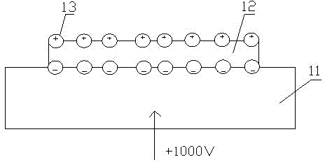
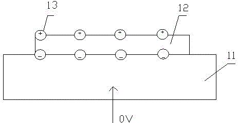
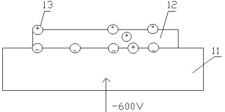
[0020] combine Figures 2a-2g As shown in , a solution to the defects of the 40 / 45 nanometer process metal hard mask structure, wherein the metal hard mask structure is to sequentially deposit the first dielectric layer 22 and the second dielectric layer on the metal sheet 21 23 and a composite structure 24; the composite structure 24 is divided into three layers, which are the first layer, the second layer, and the third layer from top to bottom; in one embodiment of the present invention, the metal sheet 21 is made of copper metal; The first dielectric layer 22 is a relatively high dielectric constant dielectric layer, the second dielectric layer 23 is an ultra-low dielectric constant dielectric layer, the composite structure 24 adopts the second layer as a TiN metal hard mask, the first lay...


PUM


Abstract

The invention relates to a defect solving means for a metal hard photomask structure, and particularly relates to a defect solving means for a metal hard photomask structure in 40 / 45 nanometer technology. According to the defect solving means for a metal hard photomask structure in 40 / 45 nanometer technology, after the etching of a composite structure, a plasma silicon wafer desorption method is used instead of the traditional direct-current silicon wafer desorption method to remove charges remaining on the surface of the composite structure due to etching, thereby solving the problem of metal-induced power failure caused by residual charge adsorption defect and improving the production quality and efficiency.

Description

technical field [0001] The invention relates to a defect solution for a metal hard mask structure, in particular to a defect solution for a 40 / 45 nanometer process metal hard mask structure. Background technique [0002] At present, starting from the 65nm process technology, the back-end dual damascene process mostly adopts low dielectric constant or copper process plus metal hard mask layer. However, when choosing the process of metal hard mask, it will face many problems that traditional processes did not have before. The problems encountered, such as after the metal hard mask is etched, there will be residual charges on the metal surface, and the residual charges will attract defects, which are difficult to remove even in subsequent cleaning steps, eventually causing metal fractures. Wire. like Figure 1a-1c It is a schematic structural flow diagram of the existing 40 / 45 nanometer technology DC desorption silicon wafer method. Metal hard mask after etching, such as Fi...

Claims


Application Information

Patent Timeline
Patent Type & Authority Patents(China)
IPC IPC(8): H01L21/768
Inventor 张瑜黄君盖晨光
Owner SHANGHAI HUALI MICROELECTRONICS CORP
Why Eureka
Try Eureka