Preparation method of copper interconnecting layer for improving etching appearance and reliability

A technology for copper interconnection and reliability, which is used in semiconductor/solid-state device manufacturing, electrical components, circuits, etc. to improve the etching morphology and improve reliability.

Active Publication Date: 2015-01-07
SHANGHAI HUALI MICROELECTRONICS CORP
View PDF3 Cites 2 Cited by
  • Summary
  • Abstract
  • Description
  • Claims
  • Application Information

AI Technical Summary

Problems solved by technology

[0015] The present invention is aimed at the prior art, where the ultra-low dielectric constant film under the ultra-low dielectric constant protective layer is bow-shaped by adopting the traditional method, and the transition interface of the material will have obvious severe Defects in the process such as side cuts provide a copper interconnection preparation method that improves etching morphology and improves reliability

Method used


Image

  • Preparation method of copper interconnecting layer for improving etching appearance and reliability
  • Preparation method of copper interconnecting layer for improving etching appearance and reliability
  • Preparation method of copper interconnecting layer for improving etching appearance and reliability

Examples


Embodiment Construction

[0046] In order to illustrate the technical content, structural features, achieved goals and effects of the present invention in detail, the following will be described in detail in conjunction with the embodiments and accompanying drawings.

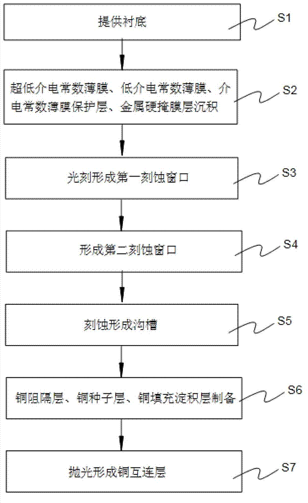
[0047] see figure 1 , figure 1 Shown is a flow chart of the copper interconnection preparation method for improving etching morphology and improving reliability of the present invention. The copper interconnect preparation method for improving etching morphology and improving reliability comprises the following steps:

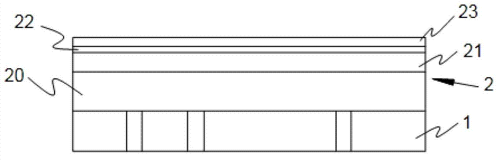
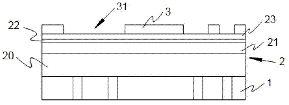
[0048]Executing step S1: providing a substrate for carrying the functional film system. For example, the functional film system sequentially includes an ultra-low dielectric constant film, a low dielectric constant film, a dielectric constant film protective layer, and a metal hard mask layer from the substrate upward;

[0049] Executing step S2: sequentially depositing an ultra-low dielectric constant film, a low di...


PUM


Abstract

A preparation method of a copper interconnecting layer for improving etching appearance and reliability comprises the following steps: S1: providing a substrate; S2: depositing a functional film system on the substrate; S3: forming a first etching window; S4: forming a second etching window; S5: etching to form a groove communicated with the substrate; S6: depositing a copper barrier layer and a copper seed layer in the groove, and forming a copper filling and depositing layer; and S7: forming a copper interconnecting layer through chemical mechanical polishing. An etched pattern prepared by the preparation method of the copper interconnecting layer for improving the etching appearance and the reliability does not have an obvious jump; a side cutting phenomenon of a transitional interface of an ultralow dielectric constant film and a low dielectric constant film is not obvious; and the covering quality of the copper barrier layer and the copper seed layer of the copper interconnecting layer prepared by the preparation method of the copper interconnecting layer for improving the etching appearance and the reliability is improved, thus further improving the reliability of a semiconductor device.

Description

technical field [0001] The invention relates to the technical field of semiconductor devices, in particular to a copper interconnect preparation method for improving etching morphology and improving reliability. Background technique [0002] With the continuous advancement of VLSI process technology, the feature size of semiconductor devices continues to shrink, and the chip area continues to increase. We are faced with the problem of how to overcome the significant increase in RC delay caused by the rapid increase in connection length. In particular, due to the increasing influence of the capacitance between metal wiring lines, the performance of the device is greatly reduced, which has become a key restrictive factor for the further development of the semiconductor industry. [0003] In order to reduce the RC delay caused by interconnection, various measures have been adopted. One of these is the use of ultra-low-k (Ultra-low-k) materials to reduce parasitic capacitance b...

Claims


Application Information

Patent Timeline
Patent Type & Authority Patents(China)
IPC IPC(8): H01L21/768
Inventor 陈玉文胡友存李磊姬峰梁学文
Owner SHANGHAI HUALI MICROELECTRONICS CORP
Why Eureka
Try Eureka