
Growth technology for growing high-quality GaN crystal material on sapphire patterned substrate

A technology for patterning substrates and sapphire substrates, applied in the field of physical and chemical growth technology, can solve problems such as weak control ability, difficulty in obtaining high-quality GaN materials, and limitations

Inactive Publication Date: 2012-12-05
姜涛
View PDF0 Cites 8 Cited by
  • Summary
  • Abstract
  • Description
  • Claims
  • Application Information

AI Technical Summary

Problems solved by technology

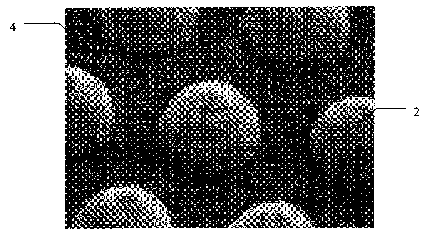
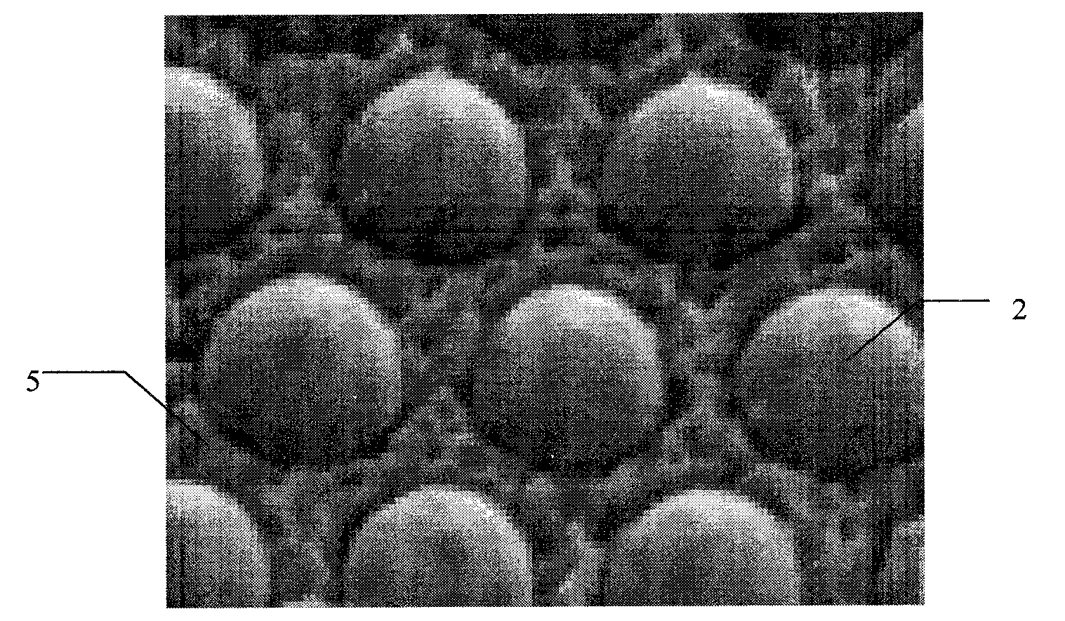
[0004] The PSS substrate adopts the etching process to process platform protrusions or conical protrusion distributions on the surface of a smooth Al2O3 substrate (such as figure 1 shown), and then epitaxially grow GaN material on the basis of this pattern, which will bring GaN material not only to grow on the 0001 plane perpendicular to the plane direction of the substrate material, but also on the side of the exposed protrusion pattern (non-0001 direction), as the material layer growth thickness increases, a flat GaN material layer surface will eventually be obtained for the subsequent growth of device structures such as LEDs, but in the planarization process of GaN material growth, due to the The material growing perpendicular to the side and the material growing perpendicular to the horizontal direction will intersect and merge with each other, and the material growing perpendicular to the horizontal direction between the protrusions will also merge with each other after reaching a certain thickness. This mutual combining process will produce various growth defects. and stress, which to some extent limits the quality of GaN material that can be obtained by growing GaN material on PSS substrates
[0005] The technology currently used is based on the growth of GaN material on a smooth Al2O3 substrate, by increasing the growth time of the nucleation layer and buffer layer, using GaN thicker than the GaN material layer grown on a smooth Al2O3 substrate material layer to obtain a flat GaN layer surface, this method has weak control over the defects caused by the combination of materials grown in different directions, and is also ineffective in solving the stress release of the GaN material layer, so it is difficult to obtain high-quality GaN material

Method used


Image

  • Growth technology for growing high-quality GaN crystal material on sapphire patterned substrate
  • Growth technology for growing high-quality GaN crystal material on sapphire patterned substrate
  • Growth technology for growing high-quality GaN crystal material on sapphire patterned substrate

Examples


Embodiment Construction

[0021] The realization process of the technical scheme of the present invention is: heating the substrate material temperature to 470-570° C. and feeding Ga element MO source and NH3 as N source to grow GaN crystal nucleation layer material. The typical thickness of the nucleation layer growth is 0.5 microns. After the growth of the nucleation layer is completed, stop feeding the Ga element MO source and quickly raise the temperature of the substrate material to 980-1090 ° C. During this process, the flow of NH3 is still kept constant. The recrystallization growth of GaN crystal is carried out by Ga element MO source. The recrystallization growth process is a process of GaN material growth and decomposition at the same time. Typical values ​​for the growth time are 2 to 3 times the time to grow the first nucleation layer.

[0022] After the first recrystallization process is over, stop feeding the Ga element MO source and quickly cool down the substrate material to 470-570 °C...


PUM


Abstract

The invention discloses a growth technology for growing a high-quality GaN crystal material on a sapphire patterned substrate. The growth technology comprises the following step of: using MOCVD (metal organic chemical vapor deposition) equipment to grow a GaN crystal on the sapphire substrate. The growth technology is characterized in that a nucleating layer material of the GaN crystal is grown at a low temperature on the substrate, and the re-crystallization growth of the GaN crystal is carried out after the temperature of a substrate material is risen after the growth of a nucleating layer is completed. After a crystallization procedure is terminated, the temperature of the substrate material is reduced, and the nucleation growth of the GaN crystal, namely the three-dimensional growth of the GaN crystal, is carried out again. After a re-nucleation procedure is terminated, the temperature of the substrate material is risen again to carry out the re-crystallization growth of the GaN crystal. After the growth in each step above is completed, the temperature of a substrate slice is risen, and meanwhile, the pressure of a reaction chamber is reduced to carry out the growth of the GaN crystal material, so that a GaN material layer which has a flat surface and is further high in quality can be obtained. By using a process of combining two-time low-temperature nucleating layer growth with a high-temperature re-crystallization procedure, which is adopted in the growth technology, compared with a conventional single-time nucleating layer growth process, the GaN material with a lower defect concentration and lower material stress can be obtained.

Description

technical field [0001] The invention belongs to the technical field of compound semiconductor crystal growth, in particular to a physical and chemical growth technology for growing high-quality GaN crystal material on a sapphire (Al2O3) patterned substrate (PSS). This technology uses MOCVD equipment to grow GaN crystals on sapphire patterned substrate materials, which can effectively improve the material properties of GaN crystals, reduce the defect density of crystals and reduce the stress of crystal materials. Making light-emitting diode (LED) devices or semiconductor laser (LD) devices on the basis of GaN crystal materials obtained by this technology is more conducive to the improvement of device performance. The technology involved in the present invention is not limited to growing high-quality GaN crystal materials on sapphire patterned substrates, and can also be applied to other substrate materials such as smooth surface sapphire (Al2O3) substrates, SiC substrates, GaN ...

Claims


Application Information

Patent Timeline
IPC IPC(8): C30B29/40C30B25/16C30B25/18
Inventor 姜涛
Owner 姜涛
Learn More