Double data rate (DDR) signal wiring encapsulation substrate and DDR signal wiring encapsulation method
A signal wiring and packaging substrate technology, applied in the field of DDR signal wiring packaging substrate, can solve the problems affecting DDR high-speed signal signal integrity, fast current reversal rate, high transmission rate, etc., to achieve shortened return current path, good impedance control, and reduced The effect of small loop inductance
- Summary
- Abstract
- Description
- Claims
- Application Information
AI Technical Summary
Problems solved by technology
Method used
Image
Examples
no. 1 example
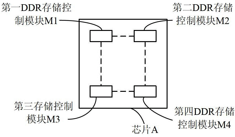
[0031] figure 1 It schematically shows the arrangement of the DDR storage control module on the DDR signal wiring package substrate according to the first embodiment of the present invention.
[0032] Such as figure 1 As shown, the DDR signal wiring packaging substrate according to the first embodiment of the present invention includes: a plurality of DDR storage control modules placed symmetrically on chip A of the DDR signal wiring packaging substrate. In this embodiment, the multiple DDR storage control modules include a first DDR storage control module M1, a second DDR storage control module M2, a third DDR storage control module M3, and a fourth DDR storage control module M4, wherein the first DDR storage The control module M1 , the second DDR storage control module M2 , the third DDR storage control module M3 and the fourth DDR storage control module M4 are located at the four corners of a square, thus forming a perfect symmetrical arrangement.
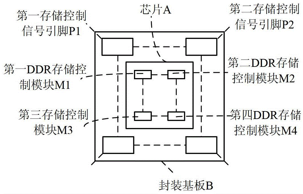
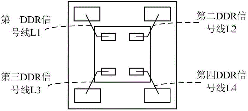
[0033] figure 2 It s...
no. 2 example
[0042] Figure 4 The layout of the DDR signal layer of the DDR signal wiring package substrate according to the second embodiment of the present invention is schematically shown.
[0043] Such as Figure 4 As shown, the DDR signal wiring package substrate according to the second embodiment of the present invention includes: a sequentially stacked ground plane layer 1, a first dielectric layer 2, a DDR signal layer 3, a second dielectric layer 4, and a DDR interface power plane layer 5 . Wherein, the DDR interface power plane layer 5 and the ground plane layer 1 are selected as the reference plane layer of the DDR signal at the same time.
[0044] On the DDR signal wiring package substrate according to the second embodiment of the present invention, a stacked structure such as the DDR interface power plane layer / DDR high-speed signal / ground plane layer is adopted, and the DDR interface power plane layer and the ground plane layer are selected as the DDR The reference plane l...
no. 3 example
[0047] Figure 5 A DDR signal wiring package substrate according to a third embodiment of the present invention is schematically shown.
[0048] The DDR signal wiring package substrate according to the third embodiment of the present invention further includes: a plurality of DDRs formed by correspondingly connecting one of the plurality of DDR storage control modules to one of the plurality of storage control signal pins. Signal vias.
[0049] The DDR signal wiring package substrate according to the third embodiment of the present invention further includes: a plurality of ground holes arranged symmetrically with reference to the positions of the plurality of DDR signal via holes.
[0050] More specifically, in this embodiment, the first DDR signal via hole W1, the second DDR signal via hole W2, the third DDR signal via hole W3 and the fourth DDR signal via hole W4 are formed; correspondingly refer to the first The positions of the DDR signal via hole W1, the second DDR sig...
PUM
 Abstract
Description
Claims
Application Information
 - R&D
- Intellectual Property
- Life Sciences
- Materials
- Tech Scout
- Unparalleled Data Quality
- Higher Quality Content
- 60% Fewer Hallucinations
Browse by: Latest US Patents, China's latest patents, Technical Efficacy Thesaurus, Application Domain, Technology Topic, Popular Technical Reports.
© 2025 PatSnap. All rights reserved.Legal|Privacy policy|Modern Slavery Act Transparency Statement|Sitemap|About US| Contact US: help@patsnap.com


