Double-broadband near infrared absorber

A near-infrared and absorber technology, applied in the direction of instruments, optical components, optics, etc., can solve the problems of reduced repeatability, small size and area, and high production cost, and achieve large-area production integration, broad application prospects, and easy integration Effect

Inactive Publication Date: 2012-11-28
NANJING UNIV
View PDF3 Cites 12 Cited by
  • Summary
  • Abstract
  • Description
  • Claims
  • Application Information

AI Technical Summary

Problems solved by technology

This type of absorber has complex structural design, small size and area, and high manufacturing cost
Researchers at home and abroad broaden the near-infrared absorption bandwidth by combining resonant units with different resonance frequency bands to obtain multiple absorption bands, but this further increases the difficulty of the manufacturing process and reduces the repeatability of production, which limits the use of such absorbers. Practicality
At present, in the pursuit of broadband localized plasmon resonance near-infrared perfect absorber research, the plasmon resonance structure with inherent broadband resonance absorption characteristics has not been proposed and researched and applied.

Method used


Image

  • Double-broadband near infrared absorber
  • Double-broadband near infrared absorber
  • Double-broadband near infrared absorber

Examples


Embodiment 1

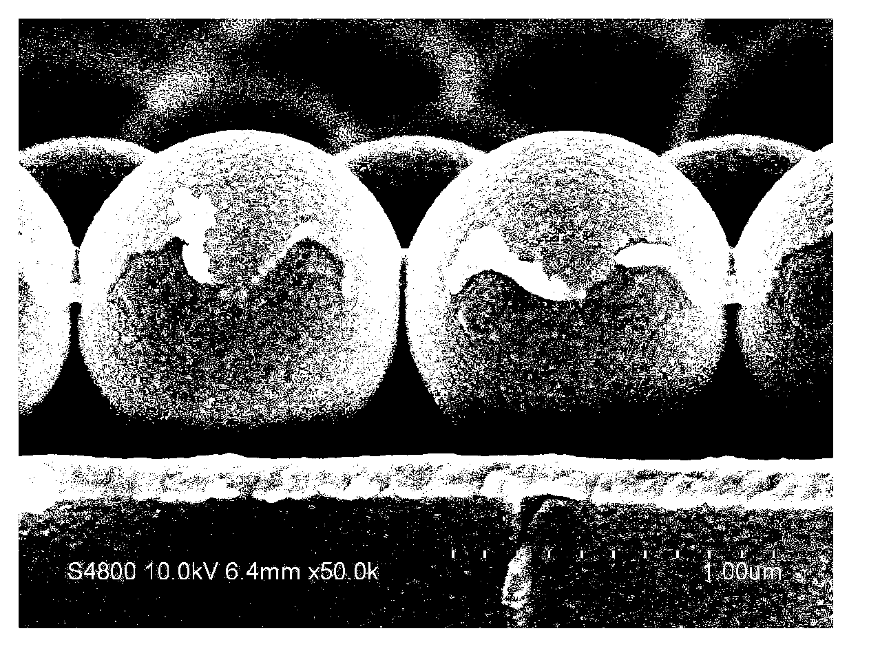
[0025] see figure 1 , the present embodiment selects monodispersed polystyrene microspheres (i.e. dielectric spheres) with a diameter of 1100 nanometers; first, a gold film with a thickness of 100 nanometers is deposited on a quartz substrate by the method of argon ion sputtering coating; Secondly, two-dimensional hexagonal close-packed dielectric spheres were assembled on the gold film substrate; then, a layer of 9-nm thick dielectric spheres was directly deposited on the surface of the two-dimensional hexagonal close-packed dielectric spheres by argon ion sputtering coating. Gold film;

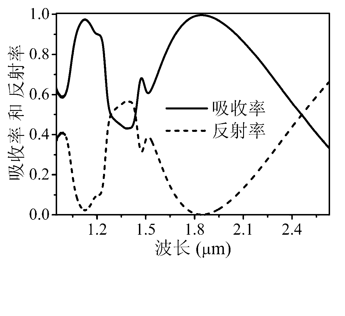
[0026] see figure 2 , the experimental results show that the double-broadband near-infrared absorber exhibits absorption rates of 97.5% and 99.6% at wavelengths of 1.120 microns and 1.841 microns, respectively;

[0027] see Figure 4 and Figure 5 , the experimental results show that the double-broadband near-infrared absorber presents perfect double-broadband near-infrared absorption w...

Embodiment 2

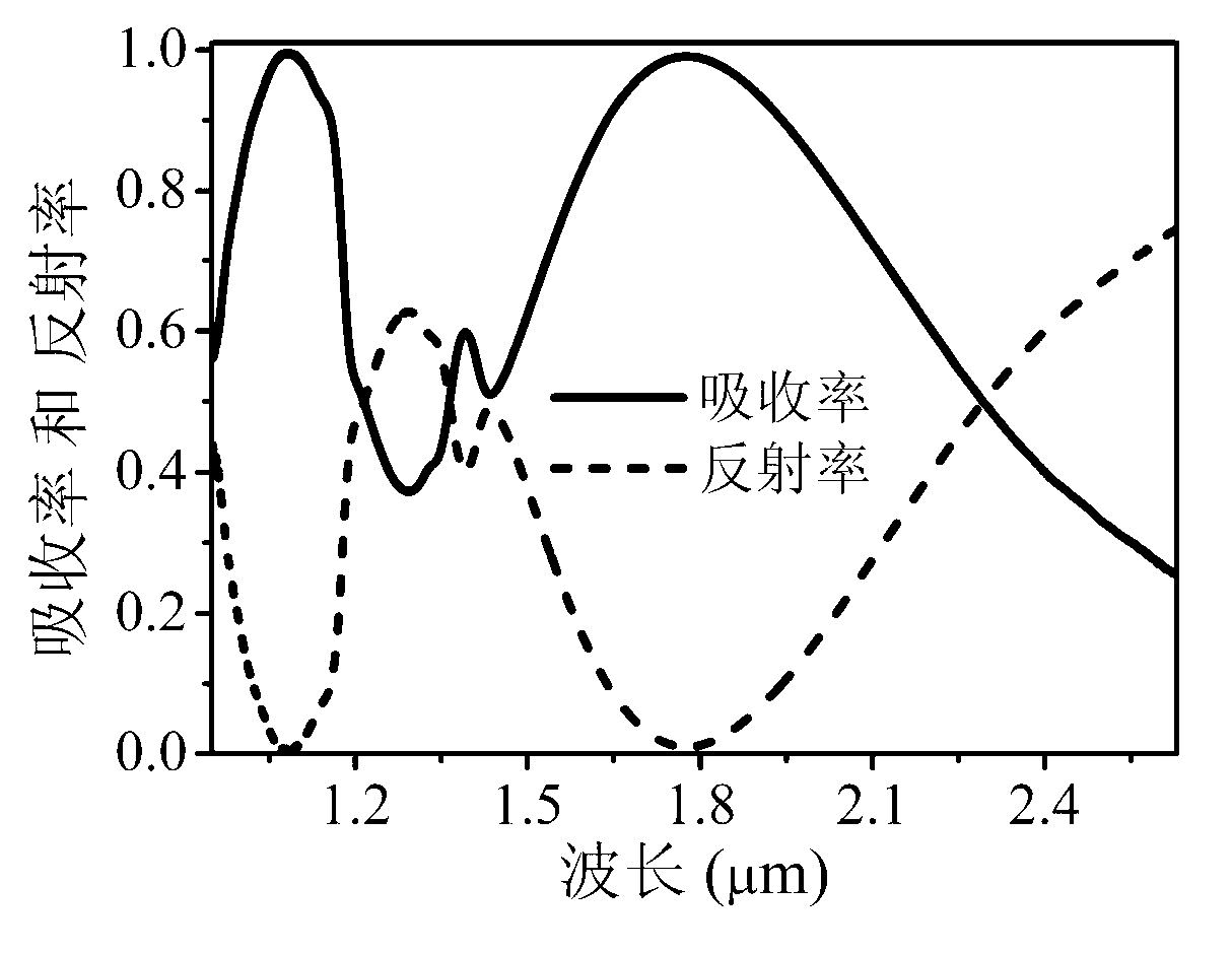
[0029] The present embodiment selects monodisperse polystyrene microspheres, and its diameter is 1000 nanometers; First adopt the method of argon ion sputtering film deposition on the quartz substrate to be the gold film of 100 nanometers in thickness; Secondly, in this gold film Assemble two-dimensional hexagonal close-packed dielectric spheres on the substrate; then use argon ion sputtering coating method to directly deposit a layer of gold film with a thickness of 9 nanometers on the surface of the two-dimensional hexagonal close-packed dielectric spheres;

[0030] see image 3 , the experimental results show that the double broadband near-infrared absorber exhibits absorption rates of 99.5% and 99.1% at wavelengths of 1.085 microns and 1.773 microns, respectively.

Embodiment 3

[0032] The present embodiment selects monodisperse polystyrene microspheres, and its diameter is 1100 nanometers; First adopt the method of argon ion sputtering coating on the glass substrate to deposit one layer of thickness to be the gold film of 100 nanometers; Secondly, in this gold film Two-dimensional hexagonal close-packed dielectric spheres are assembled on the substrate; then a gold film with a thickness of 12 nanometers is directly deposited on the surface of the two-dimensional hexagonal close-packed dielectric spheres by argon ion sputtering coating.


PUM


Abstract

The invention discloses a double-broadband near infrared absorber which comprises a substrate, wherein a first metal film layer with a thickness not less than 100 nanometers is deposited on the substrate; a single layer of dielectric spheres are densely stacked and arrayed on the first metal film layer; and a second metal film layer is deposited on the single layer of dielectric spheres. The double-broadband near infrared absorber has a perfect absorption effect on broadband near infrared electromagnetic waves which are incident by large angles, and is insensitive to polarization characteristics of the near infrared electromagnetic waves. In practical use, as the electromagnetic environment is complicated, oblique incident waves are more common than normal incident waves and incident waves with various polarization characteristics are more common than incident waves with a single polarization characteristic, the double-broadband near infrared absorber provided by the invention can be favorably adapted to the complicated electromagnetic environment. The double-broadband near infrared absorber provided by the invention has the advantages of being simple in preparation process, low in cost, high in repeatability and large-scale in production, and has a large application prospect in the field of electromagnetic energy absorption, detection, conversion and the like.

Description

technical field [0001] The invention relates to a double-broadband near-infrared absorber, specifically a new type of double-broadband near-infrared electromagnetic wave perfect absorption structure, which can be used in the fields of near-infrared electromagnetic wave absorption, detection, thermal radiation instrument and the like. Background technique [0002] The traditional near-infrared electromagnetic wave artificial electromagnetic material (Meta materials) perfect absorber is based on a narrow-band resonance absorption of a single frequency band generated by a single-size plasmon resonance structure, and based on two or more complex plasmon resonance structures of different sizes. Resonant absorption of two or more discrete frequency bands. This type of absorber has complex structural design, small size and area, and high manufacturing cost. Researchers at home and abroad broaden the near-infrared absorption bandwidth by combining resonant units with different reso...

Claims


Application Information

Patent Timeline
Patent Type & Authority Applications(China)
IPC IPC(8): G02B5/00
Inventor 刘正奇王振林詹鹏谌静
Owner NANJING UNIV
Why Eureka
Try Eureka