


Quick Research
Generate reliable direction feasibility study reports for your R&D in just a few steps.

Technical Q&A
Discover and master advanced knowledge NOW. Basics, ideas, possibilities, all at once.

Find Solutions
As an expert in R&D theories, this can generate solutions to your technical problems instantly.

Evaluate Feasibility
Analyze your overall solution with one click, know your potential R&D risks in advance.

Monitor Landscape
Get weekly tech updates, stay abreast of the latest tech innovations and key insights.
Gainp/gaas/inganas/ge four-junction solar cell and preparation method thereof
A technology of solar cells and sub-cells, applied in the field of solar cells, can solve problems affecting cell conversion efficiency, complex buffer layer growth technology, shortage of Ge materials, etc., and achieve the effects of improving cell efficiency, reducing cost and resource consumption, and reducing consumption
- Summary
- Abstract
- Description
- Claims
- Application Information
AI Technical Summary
Problems solved by technology
Method used
Image

Examples
no. 1 Embodiment approach
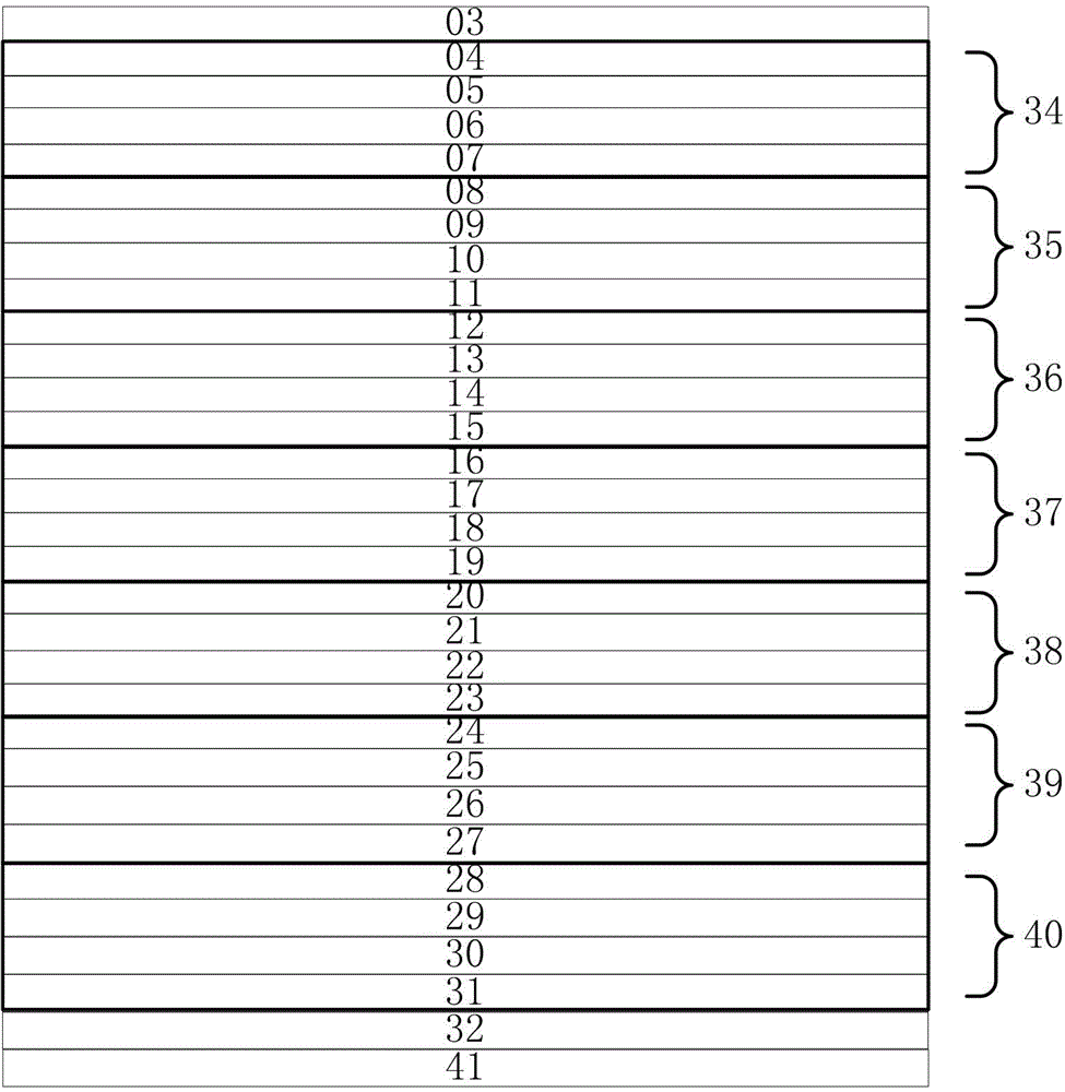
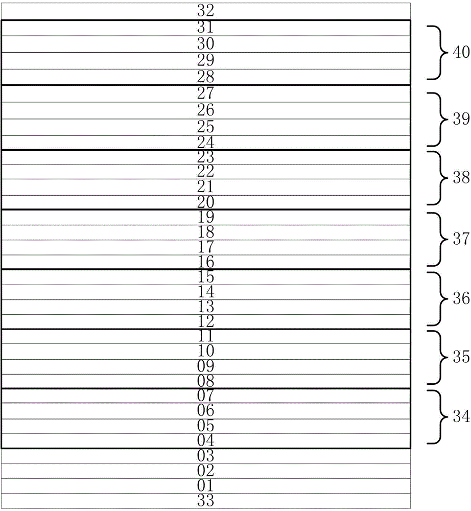
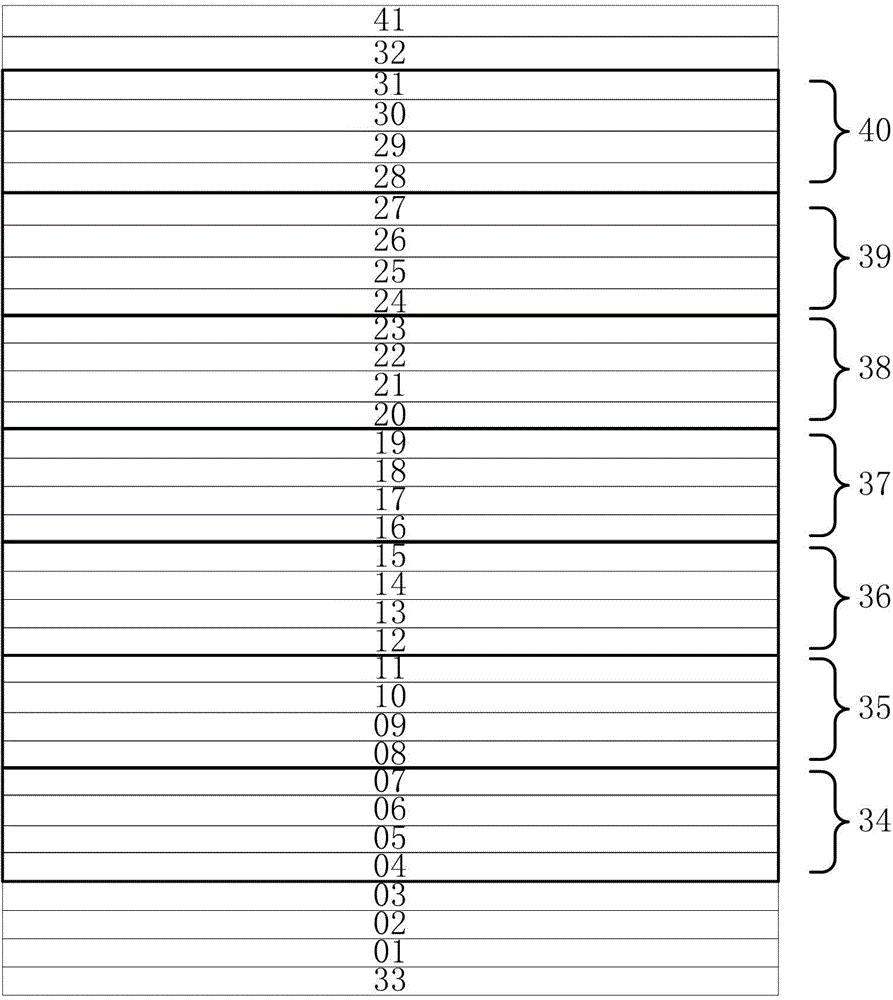
[0026] figure 1 Shown is a structural diagram of a GaInP / GaAs / InGaNAs / Ge four-junction solar cell provided in this specific embodiment.
[0027] This specific embodiment provides a GaInP / GaAs / InGaNAs / Ge four-junction solar cell, the bandgap combination is 1.90eV / 1.42eV / 1.00eV / 0.67eV, and the GaInP / GaAs / InGaNAs / Ge four-junction solar cell includes Si supporting substrate 41, and first contact layer 32 of Ge or GaInAs, Ge subcell 40, first tunnel junction 39, InGaNAs subcell 38, second tunneling junction arranged in sequence on the surface of said Si supporting substrate 41 Junction 37, GaAs subcell 36, third tunnel junction 35, GaInP subcell 34 and second contact layer 03 of InGaAs or GaAs.
[0028] As an optional implementation mode, the thickness of the second contact layer 03 of InGaAs or GaAs is in the range of 300nm to 700nm, and the doping concentration is greater than 2.0E18cm -3 .
[0029] 2.0E18cm appears in the application documents -3 Indicates 2.0×10 18 cm -3 ...
no. 2 Embodiment approach
[0046] This specific embodiment provides a method for preparing a GaInP / GaAs / InGaNAs / Ge four-junction solar cell. The bandgap combination of the solar cell is 1.90eV / 1.42eV / 1.00eV / 0.67eV, and each layer of the GaInP / GaAs / InGaNAs / Ge four-junction cell in the above manufacturing method is grown by MOCVD or MBE. If the MOCVD method is used, the N-type dopant atoms are Si, Se, S or Te, and the P-type dopant atoms are Zn, Mg or C; if the MBE method is used, the N-type dopant atoms are Si, Se, S, Sn or Te, P-type dopant atoms are Be, Mg or C.
[0047] Figure 4 It is a flow chart of the steps of the GaInP / GaAs / InGaNAs / Ge four-junction solar cell provided in this specific embodiment.
[0048] Described preparation method comprises:
[0049] Step S401, providing a GaAs substrate;
[0050] Step S402, growing the second contact layer, the GaInP sub-cell, the third tunnel junction, the GaAs sub-cell, the second tunnel junction, the InGaNAs sub-cell, the first tunnel junction, the Ge ...
PUM
 Abstract
Description
Claims
Application Information
 - R&D Engineer
- R&D Manager
- IP Professional
- Industry Leading Data Capabilities
- Powerful AI technology
- Patent DNA Extraction
Browse by: Latest US Patents, China's latest patents, Technical Efficacy Thesaurus, Application Domain, Technology Topic, Popular Technical Reports.
© 2024 PatSnap. All rights reserved.Legal|Privacy policy|Modern Slavery Act Transparency Statement|Sitemap|About US| Contact US: help@patsnap.com