Chip with electrostatic protection function

An electrostatic protection and chip technology, applied in circuits, electrical components, electric solid devices, etc., can solve the problems of the influence of finger conduction capability, the inability to guarantee the electrostatic protection performance of the chip, the influence of the electrostatic protection performance of the chip, etc., to improve the electrostatic protection performance. , saving area and improving quality

Active Publication Date: 2016-01-20
HI TREND TECH SHANGHAI
View PDF11 Cites 0 Cited by
  • Summary
  • Abstract
  • Description
  • Claims
  • Application Information

AI Technical Summary

Problems solved by technology

It can be seen that the performance of the above two improvement schemes is not ideal in practical applications.
[0008] The inventors of the present invention have found that a ring of substrate connections around the ESD protection module will affect the conduction capability of the fingers. If the fingers in the ESD protection module cannot truly achieve uniform conduction, the ESD protection performance of the chip will be affected. have an impact, therefore, although the figure 1 , figure 2 The ESD protection module shown has a reduced area, but the ESD protection performance of the chip cannot be guaranteed, and no better solution has been proposed in the prior art

Method used


Image

  • Chip with electrostatic protection function
  • Chip with electrostatic protection function
  • Chip with electrostatic protection function

Examples


Embodiment Construction

[0024] In the following description, many technical details are proposed in order to enable readers to better understand the application. However, those skilled in the art can understand that without these technical details and various changes and modifications based on the following implementation modes, the technical solution claimed in each claim of the present application can be realized.

[0025] In order to make the purpose, technical solution and advantages of the present invention clearer, the following will further describe the implementation of the present invention in detail in conjunction with the accompanying drawings.

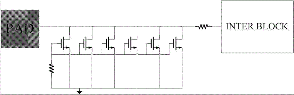
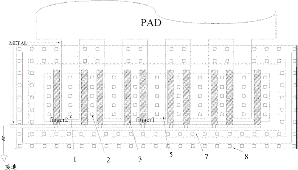
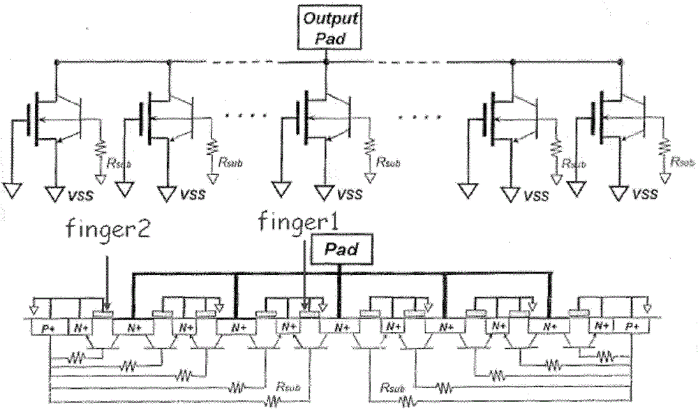
[0026] The first embodiment of the present invention relates to a chip with an electrostatic protection function. Such as Figure 8 As shown, the chip with the electrostatic protection function includes: an electrostatic protection module composed of N MOS transistors, where N is a natural number, and the electrostatic protection module is used t...


PUM


Abstract

The invention relates to an integrated circuit and discloses a chip with a static protecting function. According to the chip, in an ambient environment of a static protecting module, P+GUARD RINGs on the left side and the right side of the chip are removed and P+GUARD RINGs on the upper side and the lower side of the chip are retained. After the P+GUARD RINGs on the left side and the right side of the chip are removed, the P+GUARD RINGs seen from any one finger in the static protecting module are completely identical, so that the resistance between the finger of each MOS (Metal Oxide Semiconductor) tube in the static protecting module and the P+GUARD RINGs tends to be consistent, and further the conducting capacity of each finger in the static protecting module tends to be consistent, the MOS tubes can be uniformly conducted and the static protecting performance of the chip under the condition that the area is not increased is ensured.

Description

technical field [0001] The invention relates to an integrated circuit, in particular to a technology for improving the electrostatic protection performance of a chip. Background technique [0002] In order to prevent the chip from being damaged by static electricity from the pins and damage the internal circuit of the chip, when designing the chip, an electrostatic protection module composed of multiple metal-oxide-semiconductor (MOS) tubes is usually designed inside the chip to improve the performance of the chip. electrostatic protection performance. In order to reduce the area of ​​the electrostatic protection module as much as possible, a commonly used circuit of the electrostatic protection module connected to the pressure pad (PAD) is as follows: figure 1 As shown, the corresponding layout structure is as follows figure 2 shown. [0003] figure 1 The cross-sectional view of the ESD protection module connected to the commonly used PAD is shown in image 3 As shown...

Claims


Application Information

Patent Timeline
Patent Type & Authority Patents(China)
IPC IPC(8): H01L27/02
Inventor 曹廷代建宾赵冬芹苗跃李秋敏
Owner HI TREND TECH SHANGHAI
Why Eureka
Try Eureka