Method for etching multilayer graphene
A technology of multi-layer graphene and layer graphene, which is applied in the direction of coating, metal material coating process, and process for producing decorative surface effects, etc. It can solve the problems of graphene edge unevenness, material performance impact, independence, etc. , to achieve the effect of smooth and flat atomic scale
- Summary
- Abstract
- Description
- Claims
- Application Information
AI Technical Summary
Problems solved by technology
Method used
Image

Examples
Embodiment 1
[0028] (1) Using the method of mechanical exfoliation, using natural graphite flakes, in 300nm-SiO 2 Graphene was prepared on a p-Si substrate, and a piece of multilayer graphene with "intrinsic" steps on the surface formed directly in the preparation process was selected as the experimental object.
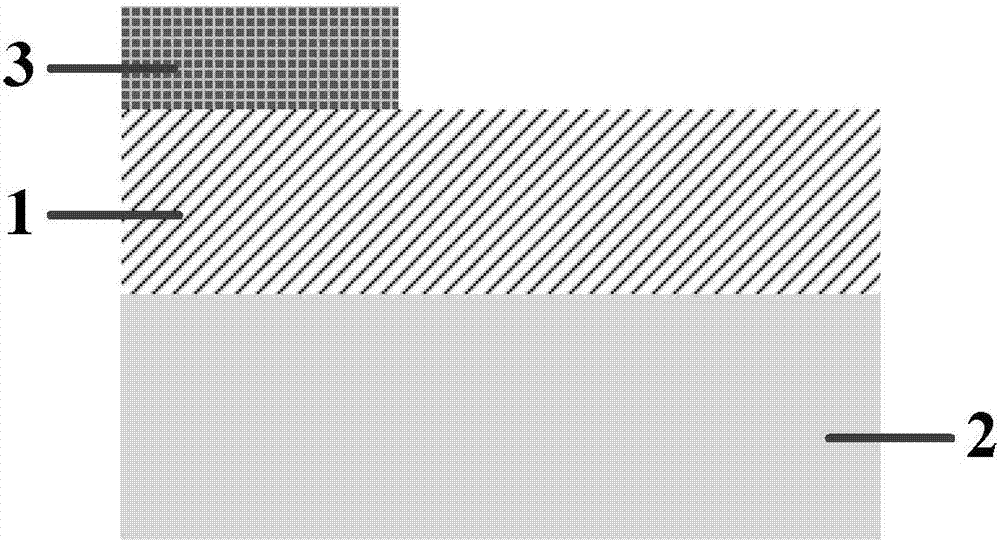
[0029] (2) Uniform thermal evaporation of 50nm Ni on the surface of the sample, in Ar / H 2 (100sccm / 10sccm) annealing at 400°C for 20 minutes in an atmosphere to form Ni particles with a diameter of about 30nm~80nm at the graphene steps;
[0030] (3) Put the sample into a high temperature tube furnace under Ar / H 2 (150sccm / 30sccm) atmosphere annealing, holding temperature at 600°C, holding time 2h, and keep Ar / H 2 The atmosphere remains unchanged until it drops to room temperature and the sample is taken out;
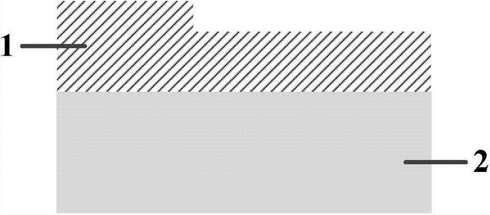
[0031] (4) Observing with a scanning electron microscope, in the step region of the multilayer graphene surface, graphene grooves etched synchronously in different layer...
Embodiment 2
[0033] (1) Using the method of mechanical exfoliation, using highly oriented graphite, in 100nm-SiO 2 Graphene was prepared on p-Si substrate.
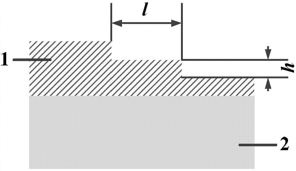
[0034] (2) According to the process steps of micro-nano processing technology to form steps, a step is formed by electron beam exposure and oxygen plasma etching, and then the exposure and etching process is repeated twice to prepare three layers on the surface of multilayer graphene. The heights are all 100 nm graphene steps, and the distance between each step is 1 μm.
[0035] (3) Spin-coat 10 mL of FeCl with a concentration of 30 mg / L on the surface of the sample 3 solution, the spin-coating speed is 2000rpm, the spin-coating time is 1min, and then in Ar / H 2 (120sccm / 15sccm) annealing at 300°C for 30 minutes in an atmosphere to form Fe particles with a diameter of about 20nm~50nm at the graphene steps;
[0036] (4) Put the sample into a high temperature tube furnace for Ar / H 2 Atmospheric annealing. Ar / H 2 The flow rates are ...
Embodiment 3
[0039] (1) CVD growth of multilayer graphene on Ni, transferred to 100nm-SiO 2 / p-Si substrate.
[0040] (2) According to the process steps of forming steps by micro-nano processing technology, a step is formed by electron beam exposure and oxygen plasma etching, and then the exposure and etching process is repeated three times, and four heights are prepared on the surface of multi-layer graphene. 80nm graphene steps, the distance between each step is 1.5μm.
[0041] (3) Using electron beam exposure and electron beam evaporation, 5nm Co was evaporated on the step formed in step (2), and after Ar / H 2 (150sccm / 10sccm) atmosphere and annealing at 350°C for 25min, Co particles with a diameter of about 10nm~30nm were formed at the graphene steps.
[0042] (4) Put the sample into a high temperature tube furnace under Ar / H 2(120sccm / 30sccm) atmosphere annealing, holding temperature at 1100°C, holding time 2.5h, and keep the atmosphere constant until it drops to room temperature, t...
PUM
| Property | Measurement | Unit |
|---|---|---|
| diameter | aaaaa | aaaaa |
Abstract
Description
Claims
Application Information
 - R&D
- Intellectual Property
- Life Sciences
- Materials
- Tech Scout
- Unparalleled Data Quality
- Higher Quality Content
- 60% Fewer Hallucinations
Browse by: Latest US Patents, China's latest patents, Technical Efficacy Thesaurus, Application Domain, Technology Topic, Popular Technical Reports.
© 2025 PatSnap. All rights reserved.Legal|Privacy policy|Modern Slavery Act Transparency Statement|Sitemap|About US| Contact US: help@patsnap.com