Method for preparing Hf-based high-K gate dielectric film on GaAs substrate
A gate dielectric and thin film technology is applied in the field of preparing Hf-based high-K gate dielectric thin films on GaAs substrates. , the effect of reducing the Fermi level pinning effect
- Summary
- Abstract
- Description
- Claims
- Application Information
AI Technical Summary
Problems solved by technology
Method used
Image
Examples
Embodiment 1
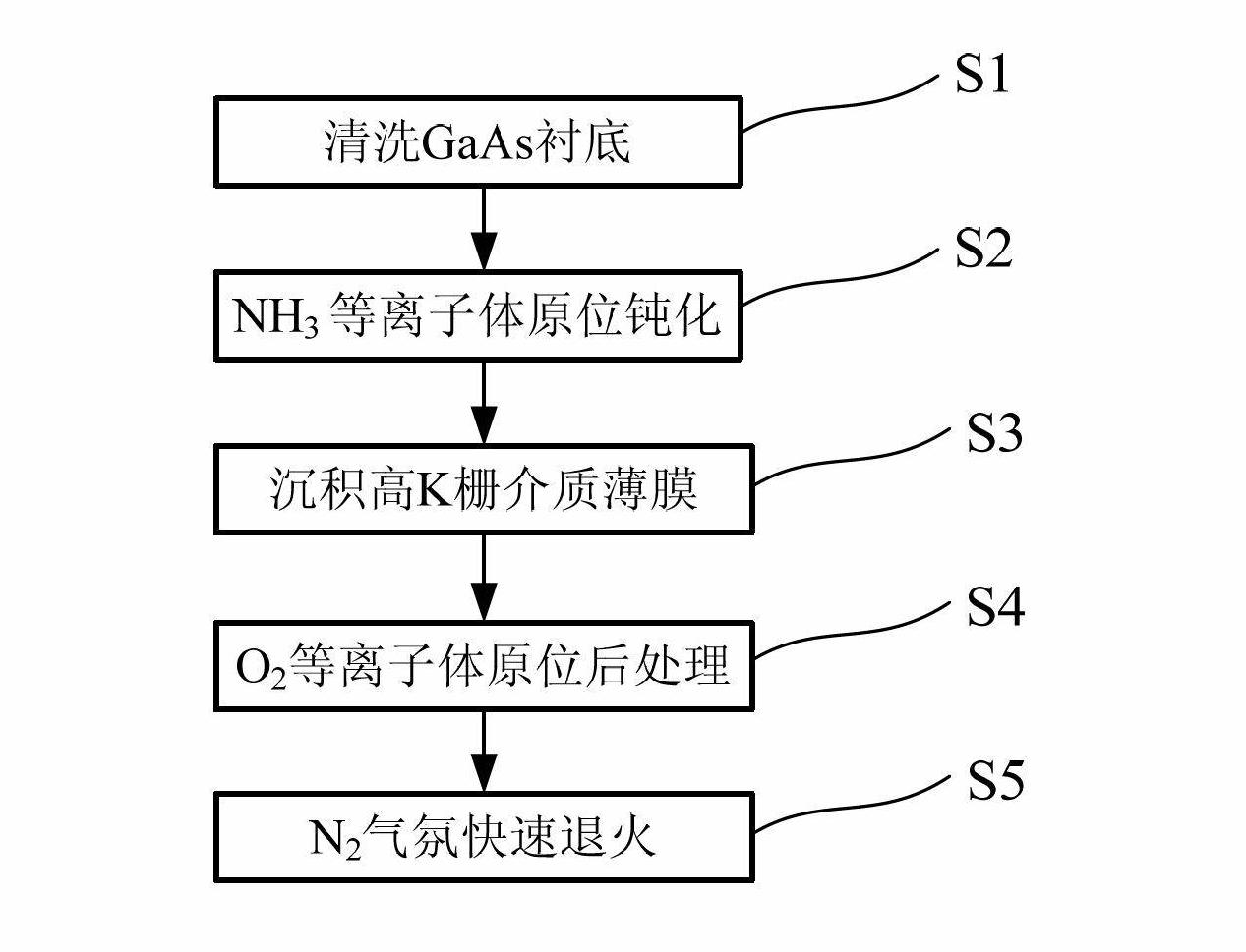
[0035] see figure 1 , which is shown as a process flow chart of preparing an Hf-based high-K gate dielectric film on a GaAs substrate in the present invention. As shown in the figure, the process method at least includes the following steps:
[0036] Step S1: Provide a single crystal GaAs wafer as the substrate substrate, and clean the GaAs substrate. The cleaning process is: first use acetone and absolute ethanol to ultrasonically clean the wafer for 3 to 5 minutes, preferably 5 minutes in this embodiment. minutes, then use 10% to 20% HCl solution to clean the GaAs surface for 1 to 5 minutes, preferably 3 minutes in this embodiment, rinse the sample with a large amount of deionized water, and finally use N 2 blow dry.
[0037] Step S2: Quickly put the dried GaAs wafer into the PEALD reaction chamber, and the GaAs wafer is exposed to the air for no more than 10 minutes. The temperature in the reaction chamber is 160°C to 250°C, preferably 180°C in this embodiment, and the ra...
Embodiment 2
[0043] Since the process flow in this embodiment is the same as that in Embodiment 1, except that the deposited high-K gate dielectric material is different, in order to simplify the description, please refer to figure 1 , the detailed steps are as follows:
[0044] Step S1: Provide a single crystal GaAs wafer as the substrate substrate, and clean the GaAs substrate. The cleaning process is: first use acetone and absolute ethanol to ultrasonically clean the wafer for 3 to 5 minutes, preferably 5 minutes in this embodiment. minutes, then use 10% to 20% HCl solution to clean the GaAs surface for 1 to 5 minutes, preferably 3 minutes in this embodiment, rinse the sample with a large amount of deionized water, and finally use N 2 blow dry.
[0045] Step S2: Quickly put the dried GaAs wafer into the PEALD reaction chamber, and the GaAs wafer is exposed to the air for no more than 10 minutes. The temperature in the reaction chamber is 160°C to 250°C, preferably 160°C in this embodi...
Embodiment 3
[0050] Since the process flow in this embodiment is the same as that in Embodiment 1, except that the deposited high-K gate dielectric material is different, in order to simplify the description, please refer to figure 1 , the detailed steps are as follows:
[0051] Step S1: Provide a single crystal GaAs wafer as the substrate substrate, and clean the GaAs substrate. The cleaning process is: first use acetone and absolute ethanol to ultrasonically clean the wafer for 3 to 5 minutes, preferably 5 minutes in this embodiment. minutes, then use 10% to 20% HCl solution to clean the GaAs surface for 1 to 5 minutes, preferably 3 minutes in this embodiment, rinse the sample with a large amount of deionized water, and finally use N 2 blow dry.
[0052] Step S2: Quickly put the dried GaAs wafer into the PEALD reaction chamber, and the GaAs wafer is exposed to the air for no more than 10 minutes. The temperature in the reaction chamber is 160°C to 250°C, preferably 200°C in this embodi...
PUM
 Abstract
Description
Claims
Application Information
 - R&D
- Intellectual Property
- Life Sciences
- Materials
- Tech Scout
- Unparalleled Data Quality
- Higher Quality Content
- 60% Fewer Hallucinations
Browse by: Latest US Patents, China's latest patents, Technical Efficacy Thesaurus, Application Domain, Technology Topic, Popular Technical Reports.
© 2025 PatSnap. All rights reserved.Legal|Privacy policy|Modern Slavery Act Transparency Statement|Sitemap|About US| Contact US: help@patsnap.com


