
Gigabit Ethernet field bus communication device based on FPGA

A Gigabit Ethernet and field bus technology, applied in the field of Gigabit Ethernet field bus communication devices, can solve the problem of low communication rate and achieve the effects of increased communication rate, fast response and high flexibility

Inactive Publication Date: 2012-07-18
HUAZHONG UNIV OF SCI & TECH
View PDF8 Cites 31 Cited by
  • Summary
  • Abstract
  • Description
  • Claims
  • Application Information

AI Technical Summary

Problems solved by technology

The above-mentioned fieldbus communication devices all have their own strengths, but generally there is a defect, that is, the communication rate of the fieldbus is generally lower than 100Mbps, and at present, with the development of technology and the improvement of demand, the requirements for the communication rate of the fieldbus are getting higher and higher. , generally need to be at 1000Mbps to achieve high real-time performance, the current fieldbus communication equipment has not been able to meet such requirements

Method used


Image

  • Gigabit Ethernet field bus communication device based on FPGA
  • Gigabit Ethernet field bus communication device based on FPGA
  • Gigabit Ethernet field bus communication device based on FPGA

Examples


Embodiment Construction

[0022] The present invention will be further described in detail below in conjunction with the accompanying drawings and specific embodiments.

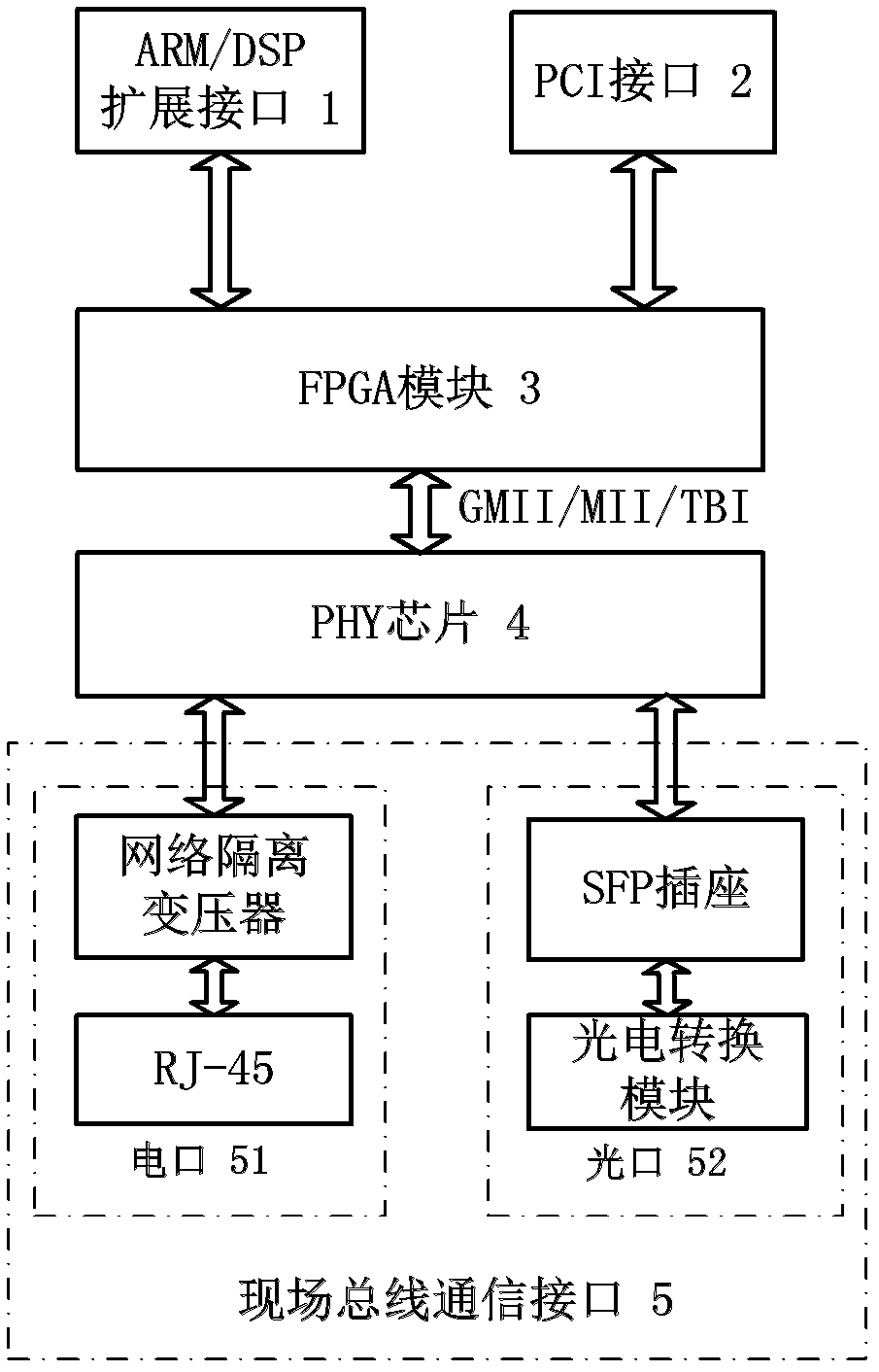
[0023] The present invention proposes an FPGA-based field bus communication device, which utilizes the programming flexibility of the FPGA to realize the control of the network card, and utilizes the Gigabit PHY chip to realize the physical layer receiving and sending data at a rate of 1000 Mbps with high real-time performance, and can expand the The interface is connected with ARM or DSP to realize functions such as monitoring and processing of bus link data and adjusting servo parameters.

[0024] figure 1 It is a schematic diagram of the overall structure of the device, which includes an ARM / DSP expansion interface 1, a PCI interface 2, an FPGA module 3, a PHY chip 4 and a field bus communication interface 5 (electrical port 51 and optical port 52).

[0025] The electrical signal or optical signal on the field bus is converted int...


PUM


Abstract

The invention discloses a gigabit Ethernet field bus communication device based on an FPGA (Field Programmable Gate Array). The device comprises an ARM (Asynchronous Response Mode) / DSP (Digital Signal Processor) expansion interface, an FPGA module, a PHY (Physical Layer) chip and a field bus communication interface and is characterized in that an electrical signal or an optical signal on a field bus is converted into a differential signal through a field bus interface; data is downloaded into the FPGA module through the gigabit PHY chip; and the FPGA module is used for receiving and analyzing the downloaded data and then transmitting the analyzed data to an ARM or a DSP connected with the ARM / DSP expansion interface through the ARM / DSP expansion interface for processing; the data processed by the ARM / DSP is packaged into a data frame by the FPGA module and is then converted into the differential signal through the gigabit PHY chip; and the differential signal is converted into the electrical signal or the optical signal through the field bus communication interface to be transmitted onto a the field bus. The gigabit Ethernet field bus communication device has the beneficial effects that the data transmission rate of 1000 Mbps can be realized, the communication with external equipment with the PCI (Peripheral Component Interconnect) interface can be realized, and different controllers can be externally connected according to the actual needs, the flexibility is high, and the gigabit Ethernet field bus communication device can be flexibly applied to real-time monitoring and communication of an industrial control field.

Description

technical field [0001] The invention belongs to the field bus communication field, and in particular relates to a Gigabit Ethernet field bus communication device, which is used for bus communication of a numerical control system. Background technique [0002] With the rapid development of computer, communication, control, electronics and other technologies, automation control quickly covers field devices in industrial systems, and fieldbus technology emerges as the times require. It interconnects on-site measurement and control equipment into a communication network, realizes information sharing between different network segments and on-site communication equipment, and at the same time transmits various information of on-site operation to the control room far away from the site, establishing a production process site level The connection between the measurement and control equipment and the control management layer. [0003] The fieldbus communication device is the core of...

Claims


Application Information

Patent Timeline
IPC IPC(8): H04L12/26H04L12/40
Inventor 宋宝唐小琦陈天航周彬马泽龙夏亮陈灏周芳芳
Owner HUAZHONG UNIV OF SCI & TECH
Learn More