Organic light emitting panel, method for manufacturing same, and organic display device
An organic light-emitting panel and a manufacturing method technology, which can be applied to lighting devices, electroluminescent light sources, semiconductor/solid-state device manufacturing, etc., can solve the problem that the thickness of the organic light-emitting layer is difficult to be uniform, and achieve good light-emitting characteristics and prevent film uneven thickness effect
- Summary
- Abstract
- Description
- Claims
- Application Information
AI Technical Summary
Problems solved by technology
Method used
Image
Examples
Embodiment approach
[0099] Hereinafter, an example of a mode for implementing the present invention will be described with reference to the drawings.
[0100] The form used in the following description is an example for explaining the structure and operation effect of this invention easily, and this invention is not limited at all by the following form except the essential characteristic part.
[0101] 1. Schematic structure of the display device 1
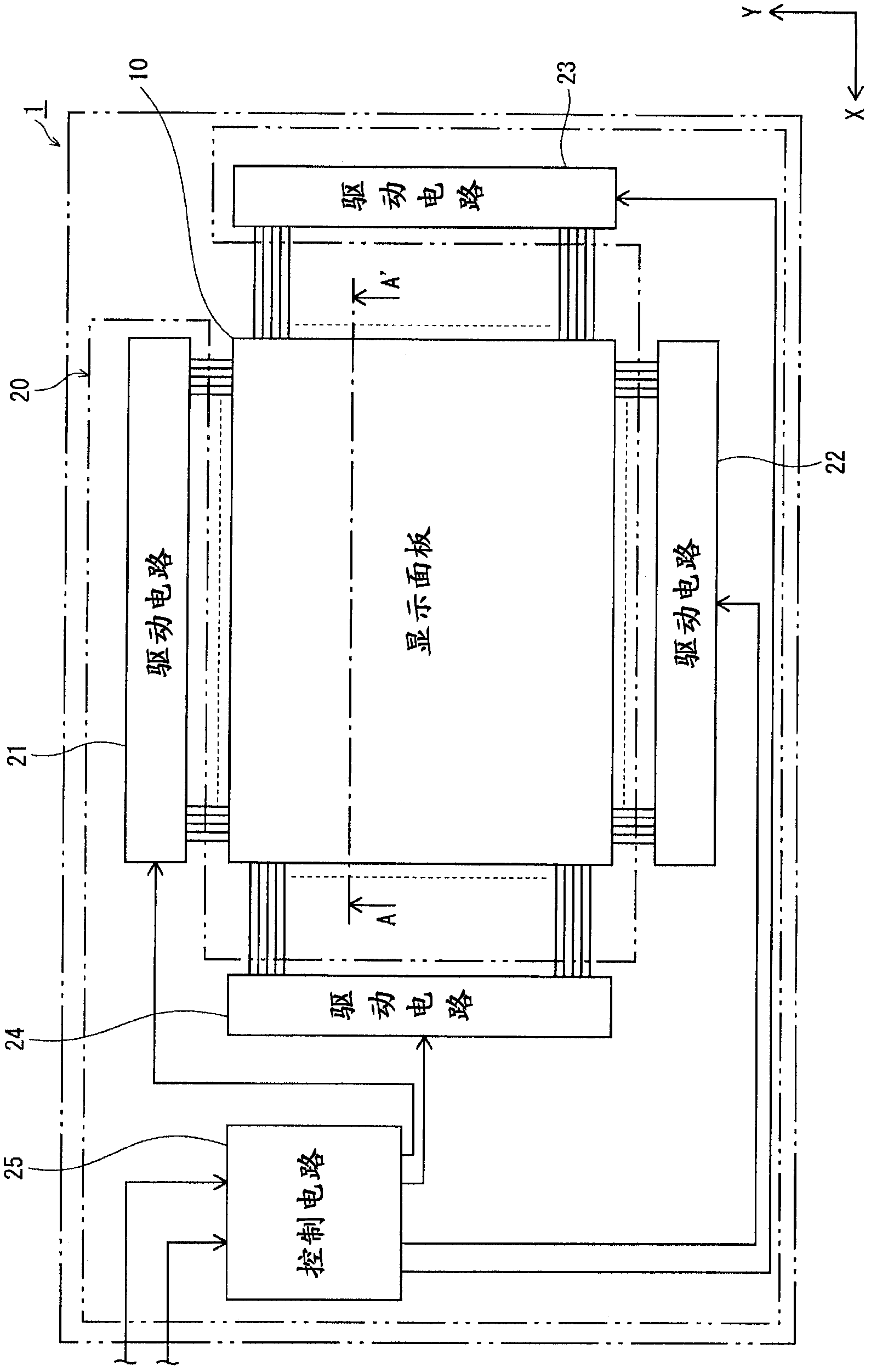
[0102] use figure 1 The overall configuration of the display device 1 according to this embodiment will be described.
[0103] Such as figure 1As shown, a display device (organic display device) 1 includes a display panel unit 10 and a drive control unit 20 connected thereto. The display panel unit 10 is an organic light-emitting panel utilizing the electroluminescence phenomenon of organic materials, and has a plurality of pixel portions arranged two-dimensionally in the X-Y plane direction.
[0104] In addition, the drive control unit 20 includ...
Deformed example 1
[0189] Next, use Figure 12 Modification 1 of the manufacturing method of the display device 1 will be described. Figure 12 express with Figure 9 (c)~ Figure 10 The process corresponding to the process shown in (a).
[0190] Such as Figure 12 As shown, after the bank material layer 1050 is laminated and formed on the hole injection transport layer 104, the mask 503 is disposed thereon. The mask 503 is provided with light-transmitting portions 503a1, 503a2, 503b, 503c, 503d1, and 503d2. The light-transmitting parts 503a1 and 503a2 are provided corresponding to the parts where the banks 105a are to be formed, the light-transmitting parts 503b and 503c are provided corresponding to the parts where the banks 105b and 105c are to be formed, and the light-transmitting parts 503d1 and 503d2 are provided corresponding to the parts where the banks 105d are to be formed. set for the location.
[0191] In the method of manufacturing the display device 1 according to Modificatio...
Deformed example 2
[0198] Next, use Figure 13 and Figure 14 Modification 2 of the manufacturing method of the display device 1 will be described. Figure 13 and Figure 14 express with Figure 9 (c)~ Figure 10 (b) The corresponding process of the process shown.
[0199] Such as Figure 13 As shown in (a), after the bank material layer 1050 is laminated and formed on the hole injection transport layer 104 , the mask 504 is disposed thereon. In the mask 504 , openings 504 a , 504 b , 504 c , and 504 d are provided corresponding to the respective locations where the banks 105 are to be formed.
[0200] The openings 504d and 504c are formed to have the same width as the openings 501b and 501c of the mask 501 used in the manufacturing method of the above-described embodiment.
[0201] On the other hand, banks 105a, 105d are formed between the planned sub-pixel region 1000a and the planned non-pixel region 1000d, and between the planned sub-pixel region 1000c and the planned non-pixel region...
PUM
 Abstract
Description
Claims
Application Information
 - R&D
- Intellectual Property
- Life Sciences
- Materials
- Tech Scout
- Unparalleled Data Quality
- Higher Quality Content
- 60% Fewer Hallucinations
Browse by: Latest US Patents, China's latest patents, Technical Efficacy Thesaurus, Application Domain, Technology Topic, Popular Technical Reports.
© 2025 PatSnap. All rights reserved.Legal|Privacy policy|Modern Slavery Act Transparency Statement|Sitemap|About US| Contact US: help@patsnap.com


