Display panel producing system and method of producing display panel
a display panel and production system technology, applied in semiconductor/solid-state device testing/measurement, instruments, optics, etc., can solve problems such as uneven front faces of substrates in production, and drawbacks, so as to prevent non-uniform display on display panels and suppress uneven thickness of films
- Summary
- Abstract
- Description
- Claims
- Application Information
AI Technical Summary
Benefits of technology
Problems solved by technology
Method used
Image
Examples
first embodiment
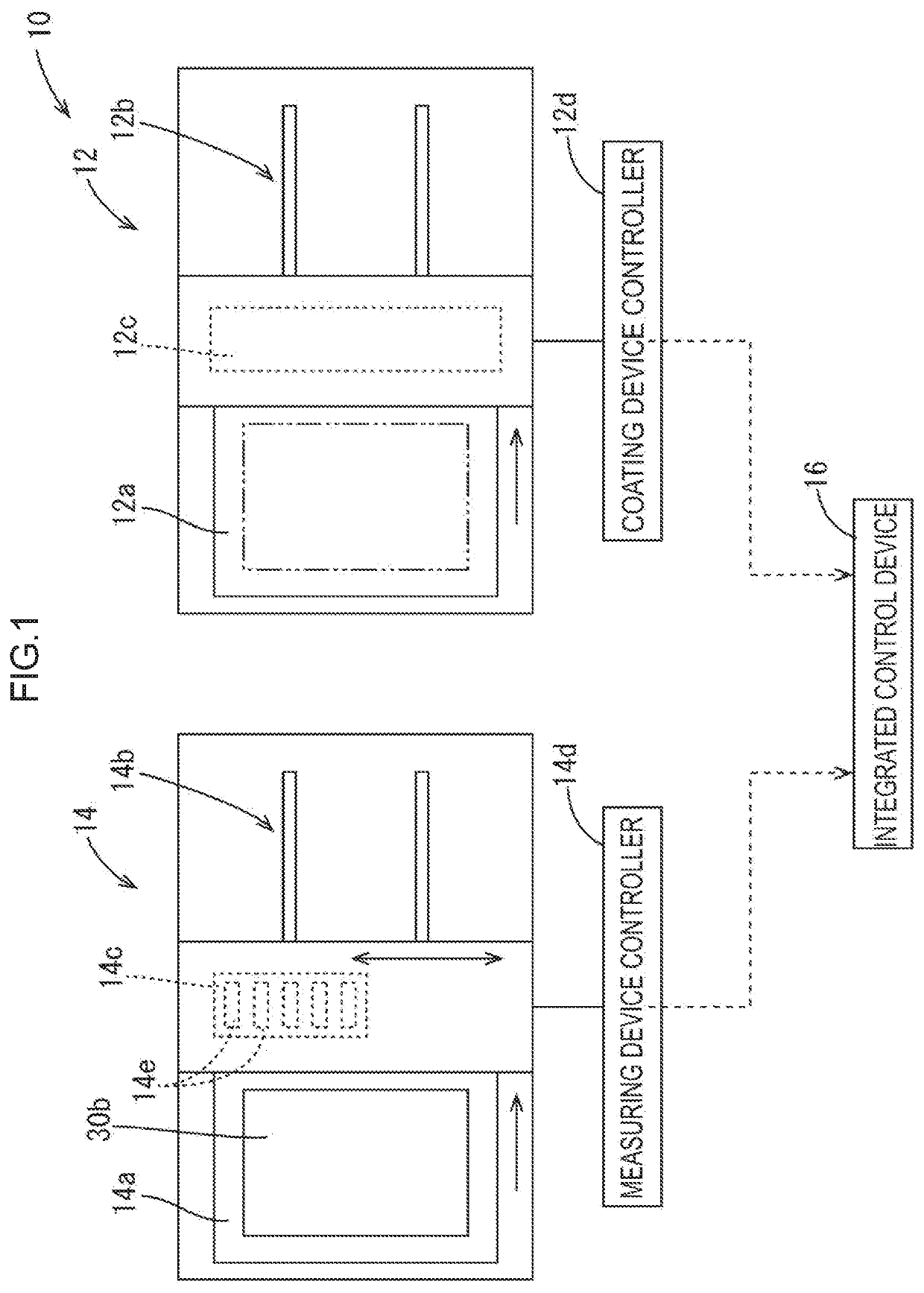
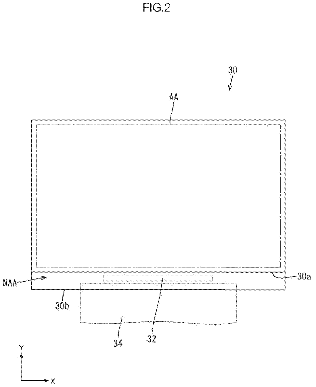
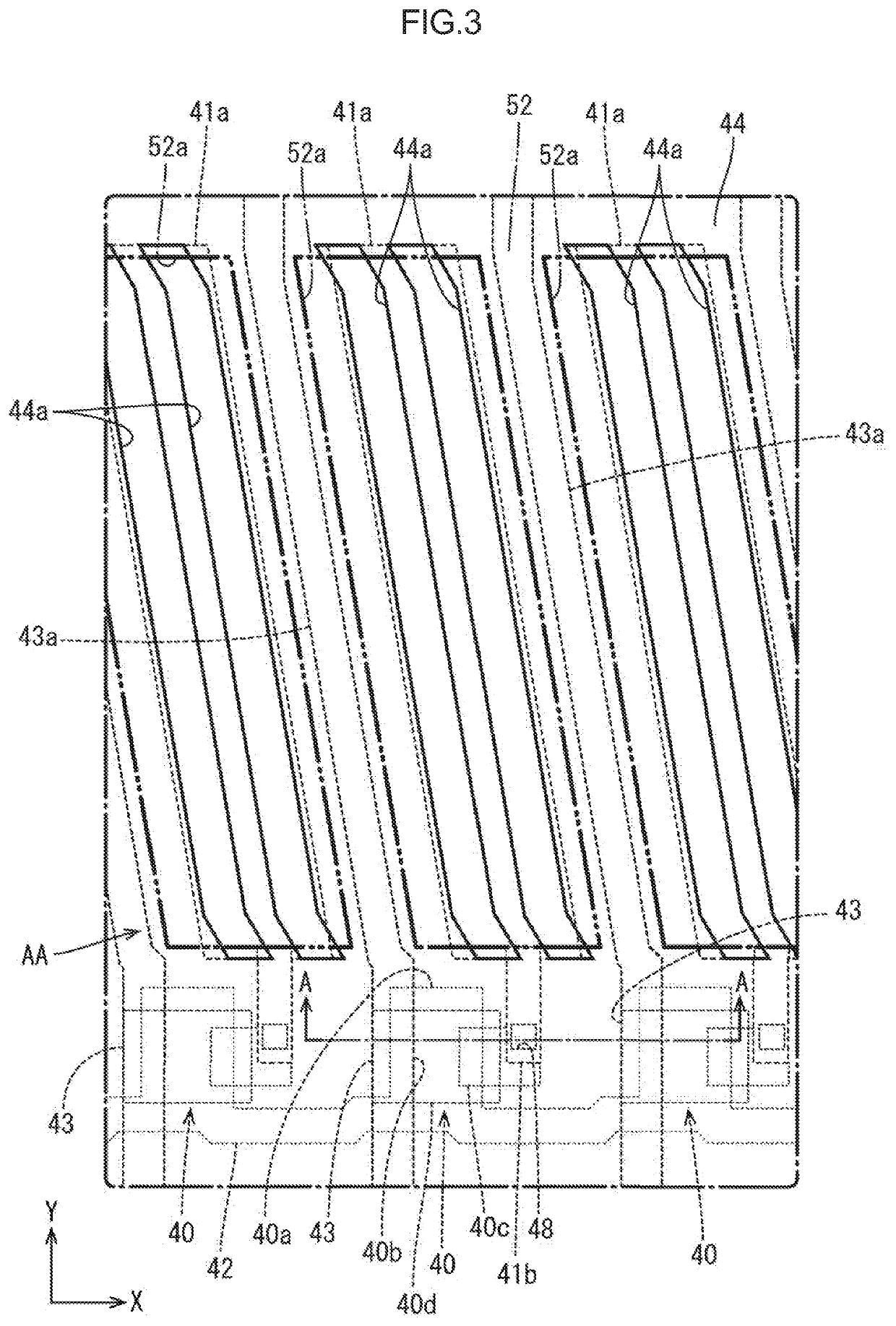
[0035]FIG. 1 schematically illustrates a display panel producing system 10 (hereinafter, simply referred to as a “producing system 10” occasionally) as a first embodiment. The producing system 10 includes an ink-jet coating device 12, a measuring device 14, and an integrated control device 16. Briefly, the producing system 10 causes the integrated control device 16 to control the ink-jet coating device 12 and the measuring device 14 integrally, and causes the ink-jet coating device 12 to perform film formation to a substrate so as to conform to an uneven shape on a front face of the substrate measured by the measuring device 14. Before detailed description is made of the producing system 10, a liquid crystal panel 30 as one example of a display panel manufactured by the producing system 10 is to be described in detail with reference to FIGS. 2 to 4.
[0036]Configuration of Display Panel
[0037]As illustrated in FIG. 2, the liquid crystal panel 30 is horizontally rectangular in its entir...
second embodiment
[0070]The display panel producing system 10 according to the first embodiment includes the ink-jet coating device 12 and the measuring device 14 individually. In contrast to this, a display panel producing system according to a second embodiment includes these units as one device. FIG. 9 illustrates a display panel producing device 80 (hereinafter, simply referred to as a “producing device 80” occasionally) as the display panel producing system in the second embodiment.
[0071]The producing device 80 conducts work similar to that of the producing system 10 in the first embodiment. That is, the producing device 80 forms the alignment film 60b of the array substrate 30b. The producing device 80 includes a base 82, a transport device 84 disposed on the base 82 for transporting a substrate S over the base 82, a frame 86 provided in the middle of the transport device 84 in a transportation direction across the transport device 84, and three work heads 88, 90, 92 provided on the frame 86 on...
PUM
| Property | Measurement | Unit |
|---|---|---|
| speed | aaaaa | aaaaa |
| viscosity | aaaaa | aaaaa |
| thickness | aaaaa | aaaaa |
Abstract
Description
Claims
Application Information
 - R&D
- Intellectual Property
- Life Sciences
- Materials
- Tech Scout
- Unparalleled Data Quality
- Higher Quality Content
- 60% Fewer Hallucinations
Browse by: Latest US Patents, China's latest patents, Technical Efficacy Thesaurus, Application Domain, Technology Topic, Popular Technical Reports.
© 2025 PatSnap. All rights reserved.Legal|Privacy policy|Modern Slavery Act Transparency Statement|Sitemap|About US| Contact US: help@patsnap.com


