High ultraviolet transmitting double-layer wire grid polarizer for fabricating photo-alignment layer and fabrication method thereof
A technology of wire grid polarization and light-controlled orientation, which is applied in polarizing elements, optics, optical elements, etc., can solve the problems of lowering the total transmittance, and achieve the effects of improving the production efficiency, increasing the degree of polarization, and increasing the transmittance
- Summary
- Abstract
- Description
- Claims
- Application Information
AI Technical Summary
Problems solved by technology
Method used
Image
Examples
preparation example Construction
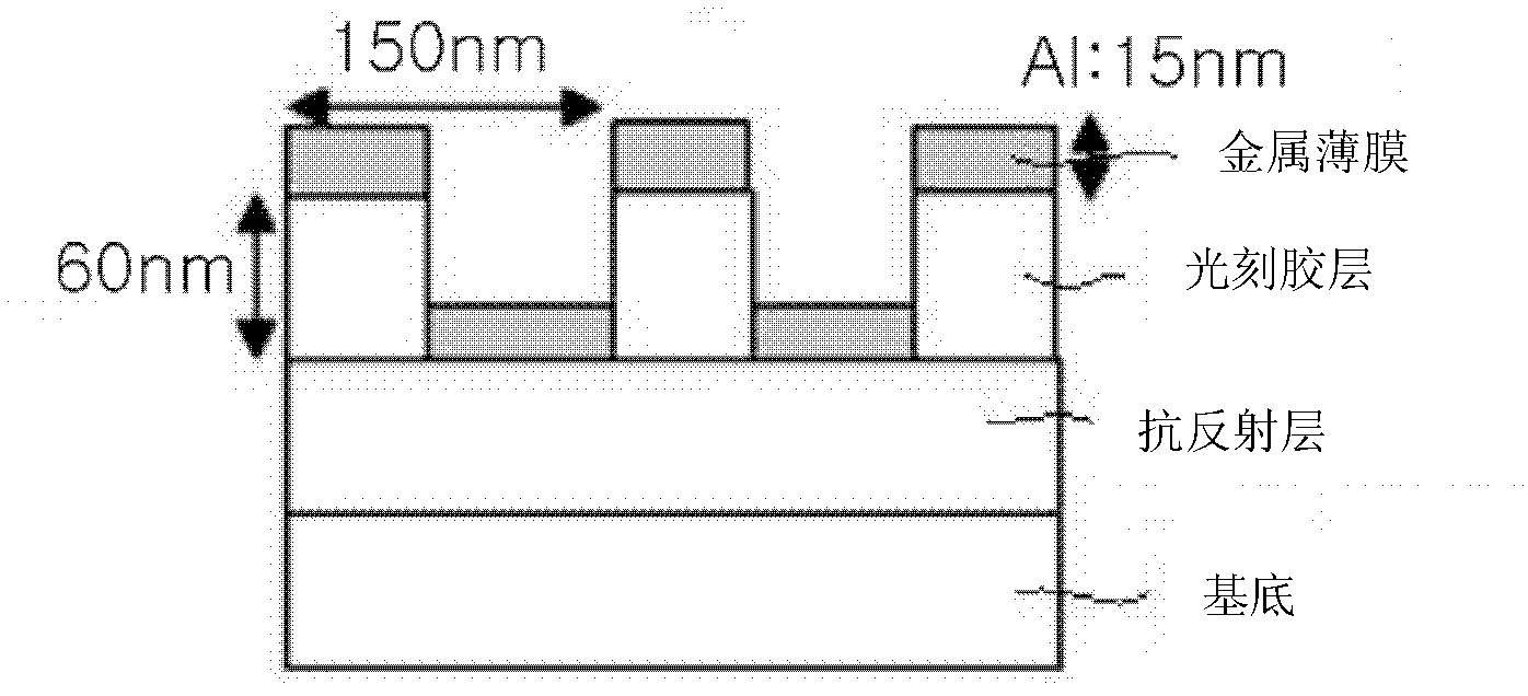
[0040]According to another aspect of the present invention, the preparation method of the ultraviolet high transmittance double-layer wire grid polarizing plate used for the photo-control alignment film comprises: forming an anti-reflection layer on the substrate (step 1); Coating photoresist on top to form a photoresist layer (step 2); selectively exposing the photoresist layer according to the pattern formed by laser interference light and developing the exposed photoresist layer to form a wire grid patterning (step 3); and depositing metal on said wire grid pattern (step 4).
[0041] Step 1 is coating an anti-reflection layer on the substrate. The substrate is an essential part of the polarizing plate, and may be made of any material as long as light can pass through the substrate. Examples of the substrate may include quartz substrates, UV-transparent glass, and plastic substrates.
[0042] The anti-reflection layer refers to the layer covered on the substrate before coa...
Embodiment 1
[0051] Example 1: Preparation of double-layer wire grid polarizer with high UV transmittance
[0052] 1. Formation of anti-reflection layer and photoresist layer
[0053] In this example, a quartz substrate with a size of 10 cm x 10 cm was used, and DUV 42p (Brewer Science) was used as the antireflection layer. Ultra i-123 (Rohm and Hass company) was used as photoresist.
[0054] A 60 nm thick antireflection layer (DUV 42p) is covered on the quartz substrate. After covering the anti-reflection layer, a 60 nm thick Ultra i-123 was coated to form a photoresist layer.
[0055] 2. Forming a wire grid pattern by laser interference exposure
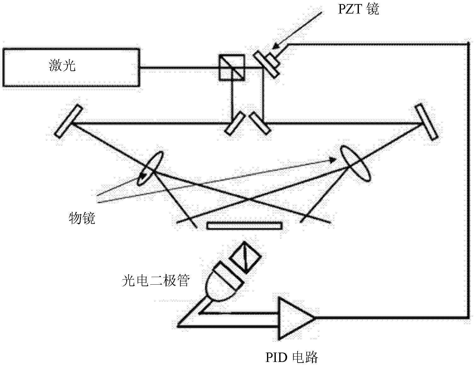
[0056] To form a wire grid pattern on the substrate prepared in Section 1 above, an interference exposure system was used. Such as figure 2 As shown, the interference exposure system uses a beam splitter to split the 266nm laser beam into two beams, and uses an objective lens to amplify these beams, and exposes the above photoresist lay...
experiment example 1
[0060] Experimental example 1: Measurement of transmittance
[0061] The transmittance was measured by using the double-layer wire grid polarizer with high ultraviolet transmittance prepared in Example 1. When randomly polarized light is incident, such as figure 1 The transmittance of the conventional single-layer polarizing plate shown in the comparative example in is 40% at a wavelength of 310 nm. The transmittance of the polarizer described in the embodiment of the present invention is 60%, which is 1.5 times of the transparency of the conventional polarizer.
PUM
| Property | Measurement | Unit |
|---|---|---|
| thickness | aaaaa | aaaaa |
| thickness | aaaaa | aaaaa |
| thickness | aaaaa | aaaaa |
Abstract
Description
Claims
Application Information
 - R&D
- Intellectual Property
- Life Sciences
- Materials
- Tech Scout
- Unparalleled Data Quality
- Higher Quality Content
- 60% Fewer Hallucinations
Browse by: Latest US Patents, China's latest patents, Technical Efficacy Thesaurus, Application Domain, Technology Topic, Popular Technical Reports.
© 2025 PatSnap. All rights reserved.Legal|Privacy policy|Modern Slavery Act Transparency Statement|Sitemap|About US| Contact US: help@patsnap.com


