Random noise source and manufacturing method thereof

A technology of random noise source and production method, applied in the fields of signal processing and cryptography, to achieve the effect of high quality and high bandwidth

Inactive Publication Date: 2012-07-11
SUZHOU INST OF NANO TECH & NANO BIONICS CHINESE ACEDEMY OF SCI
View PDF4 Cites 4 Cited by
  • Summary
  • Abstract
  • Description
  • Claims
  • Application Information

AI Technical Summary

Problems solved by technology

These methods of generating true random numbers, due to the limitation of the bandwidth of physical source electronic devices, generate random numbers at or below the Mbit / s level, and the speed can only meet the low-end needs

Method used


Image

  • Random noise source and manufacturing method thereof
  • Random noise source and manufacturing method thereof
  • Random noise source and manufacturing method thereof

Examples


Embodiment Construction

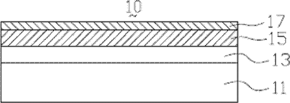
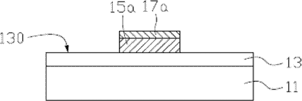
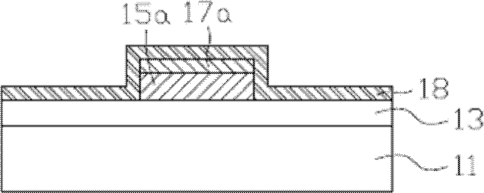
[0014] Figures 1A-1E It is a schematic diagram of the process of making a semiconductor superlattice device by semiconductor micromachining in the present invention. see Figure 1A Firstly, a semiconductor superlattice material structure 10 is provided, and the method thereof is, for example, utilizing epitaxial growth techniques such as current mainstream molecular beam epitaxy (Molecular Beam Epitaxy, MBE), metal organic chemical vapor deposition (Metal Organic Chemical Vapor Deposition, MOCVD) and doping An epitaxial growth layer is formed on the semi-insulating semiconductor substrate 11 using complex techniques. Here, the epitaxial growth layer includes a first semiconductor contact layer 13 , a semiconductor superlattice layer structure 15 and a second semiconductor contact layer 17 sequentially formed on the semi-insulating semiconductor substrate 11 . In this embodiment, the material of the epitaxial growth layer uses III-V or II-VI compound semiconductor materials, ...


PUM


Abstract

The invention relates to a random noise resource and a manufacturing method thereof. The random noise source comprises a two-end semiconductor superlattice device which is fixed on a microwave printed circuit board and electrically connected with the microwave printed circuit board, wherein the two-end semiconductor superlattice device comprises a semi-insulation semiconductor substrate, a first semiconductor contact layer, a semiconductor superlattice layer structure and a second semiconductor contact layer which epitaxially grow on the semi-insulation semiconductor substrate sequentially, a first contact electrode and a second contact electrode, wherein the first semiconductor contact layer, the semiconductor superlattice layer structure and the second semiconductor contact layer are made of compound semiconductor materials in the III-V cluster or II-VI cluster; and n-type impurities are doped in the first semiconductor contact layer, a potential well layer in the semiconductor superlattice layer structure and the second semiconductor contact layer respectively. Due to a solid automatic chaotic oscillation characteristic of the semiconductor superlattice device, the random noise resource with true randomness, high quality and high bandwidth is implemented; and flat broadband chaotic signals with bandwidths of greater than GHz are output.

Description

technical field [0001] The invention relates to the technical fields of signal processing and encryption, in particular to a random noise source and a manufacturing method thereof. Background technique [0002] Random noise source technology is an important branch of cryptography. Random noise sources and random number generators have a wide range of applications, and are indispensable key components in encryption systems and various cryptographic security systems. Its working status directly affects the reliability and stability of encryption systems and various cryptographic security systems, and the quality of the random sequences generated is related to the protection strength of cryptographic equipment for information. [0003] A random noise source is at the heart of a random number generator. True randomness, high quality, and high bandwidth are the three basic requirements for high-quality noise sources. First, a high-quality noise source requires that the signal ...

Claims


Application Information

Patent Timeline
Patent Type & Authority Applications(China)
IPC IPC(8): H03B29/00
Inventor 黄寓洋张耀辉李文
Owner SUZHOU INST OF NANO TECH & NANO BIONICS CHINESE ACEDEMY OF SCI
Why Eureka
Try Eureka