Solid state light emitting device and method for making the same

A technology of solid-state luminescence and manufacturing methods, which is applied to electrical components, semiconductor devices, circuits, etc., and can solve problems such as uncontrollable distribution, random differences, affecting wavelength range and luminous uniformity

Inactive Publication Date: 2012-05-23
LEXTAR ELECTRONICS CORP
View PDF4 Cites 2 Cited by
  • Summary
  • Abstract
  • Description
  • Claims
  • Application Information

AI Technical Summary

Problems solved by technology

[0010] It can be seen from the above description that although the luminous efficiency of the light-emitting diode 2 with a quasi-quantum dot structure is higher than that of the light-emitting diode 1 with a quantum well structure, the quasi-quantum dot 233 is formed by heat-treating a thin film of gallium indium-based compound at a high temperature. Formed from self-deformation, the shape and size are quite random with large differences, and the distribution state is also uncontrollable; according to research, the quasi-quantum dot structure is a structure that generates light energy, and its size and distribution state will affect the wavelength range of light emission. and luminous uniformity, and therefore, there is still room for improvement in the current quantum dot-like structure of light-emitting diodes, which requires the investment and efforts of the industry
[0011] It can be seen that the above-mentioned existing light-emitting diodes obviously still have inconvenience and defects in product structure, manufacturing method and use, and need to be further improved urgently.

Method used


Image

  • Solid state light emitting device and method for making the same
  • Solid state light emitting device and method for making the same
  • Solid state light emitting device and method for making the same

Examples


Embodiment Construction

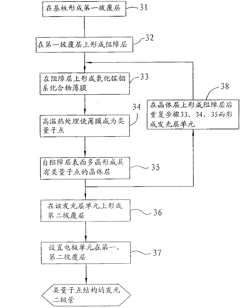
[0073] In order to further explain the technical means and effects of the present invention to achieve the intended purpose of the invention, the specific implementation of the solid-state light-emitting component with quantum cluster columns and its manufacturing method according to the present invention will be described below in conjunction with the accompanying drawings and preferred embodiments. , structure, method, step, feature and effect thereof, detailed description is as follows.

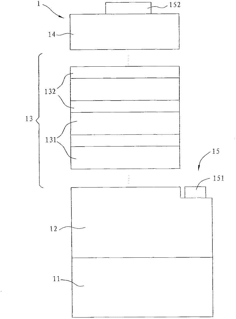
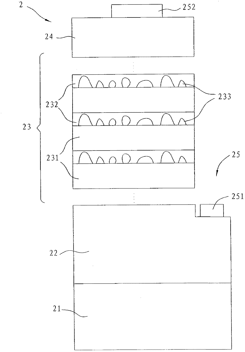
[0074] refer to Figure 4 A preferred embodiment of the solid-state light-emitting component with quantum cluster columns in the present invention includes a substrate 41, a first cladding layer 42 (n-cladding layer), a second cladding layer 44 (p-cladding layer ), a light-emitting layer unit 43 sandwiched between the first and second cladding layers 42, 44, and a set of electrode units 45 electrically connected to the cladding layers 42, 44 and an external power source.

[0075] The subs...


PUM


Abstract

A method for making a solid state light emitting device includes: (a) forming a first cladding layer (42) on a substrate (41); (b) forming a matrix layer (431) above the first cladding layer (42), the matrix layer (431) having a top surface and being formed with a plurality of isolated spaces (434); (c) epitaxially forming a quantum cluster (432) in each of the spaces (434) such that the top surface of the matrix layer (431) and top surfaces of the quantum clusters (432) cooperatively define a coplanar surface (4301), the quantum clusters (432) cooperating with the matrix layer (431) to form a light emitting layer (430); (d) forming a second cladding layer (44) on the light emitting layer (430); and (e) forming an electrode unit (45) electrically connected to the first and second cladding layers (42, 44).

Description

technical field [0001] The invention relates to a light-emitting component and a manufacturing method thereof, in particular to a solid-state light-emitting component with a quantum cluster and a manufacturing method thereof. Background technique [0002] Solid-state light-emitting components, especially light-emitting diodes (LEDs for short), are used in a wide range of fields, mainly as display backlight modules, traffic signals and lighting. With the improvement of environmental protection awareness, light-emitting diodes are actively developed as the main light source of the new generation to replace the mercury lamps and tungsten bulbs in the past due to their advantages in energy saving and low pollution. Therefore, the brightness of light-emitting diodes is getting worse Importantly, the industry and academia are also making continuous efforts to improve the luminous efficiency of light-emitting diodes. [0003] refer to figure 1 The main structure of the convention...

Claims


Application Information

Patent Timeline
Patent Type & Authority Applications(China)
IPC IPC(8): H01L33/00H01L33/06
CPCH01L33/007H01L33/08H01L33/06
Inventor 陈铭胜梁文灯
Owner LEXTAR ELECTRONICS CORP
Why Eureka
Try Eureka