Appearance detection method of quasi-monocrystalline silicon wafer

An appearance inspection, quasi-single crystal technology, applied in the field of inspection, to achieve the effect of improving the accuracy and being easy to popularize

Inactive Publication Date: 2012-05-23
SUZHOU TALESUN SOLAR TECH CO LTD
View PDF0 Cites 7 Cited by
  • Summary
  • Abstract
  • Description
  • Claims
  • Application Information

AI Technical Summary

Problems solved by technology

There are currently no cheap and convenient quantitative methods and tools to measure this proportional parameter

Method used


Image

  • Appearance detection method of quasi-monocrystalline silicon wafer
  • Appearance detection method of quasi-monocrystalline silicon wafer

Examples


Embodiment Construction

[0014] The appearance inspection method of quasi-single crystal silicon wafer is different in that it includes the following steps:
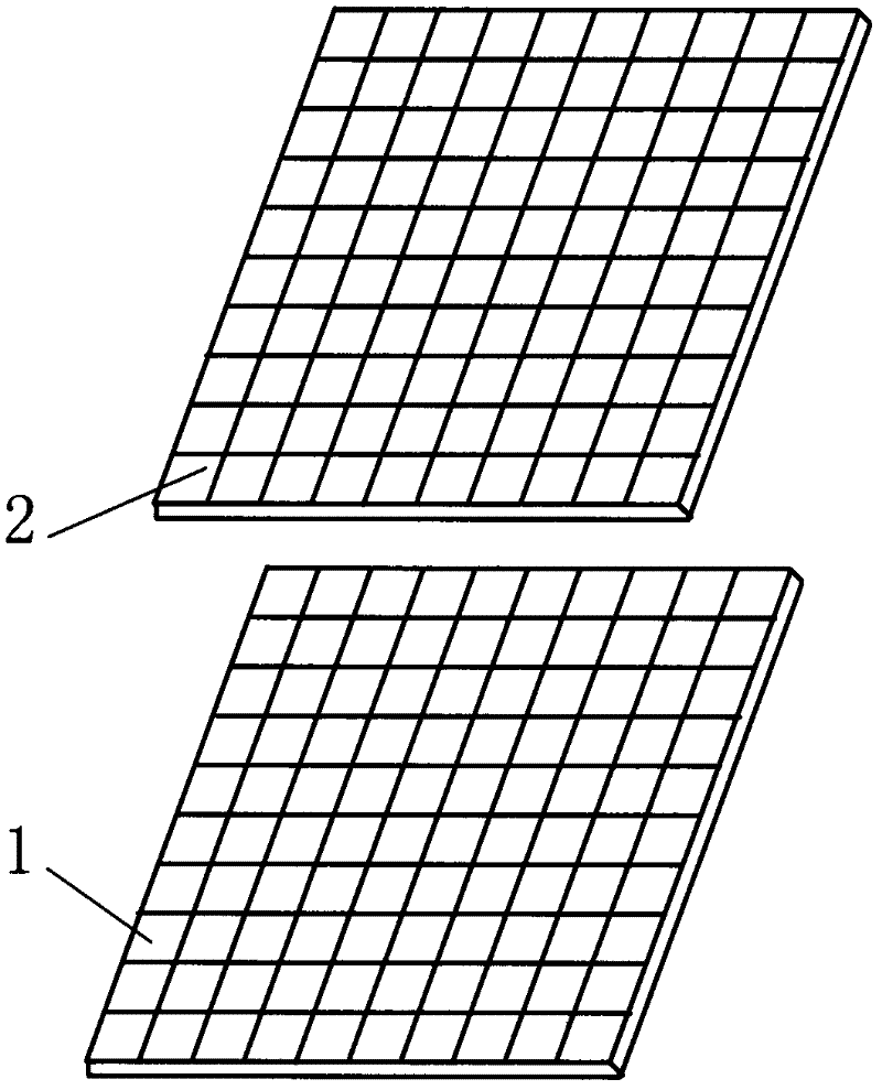
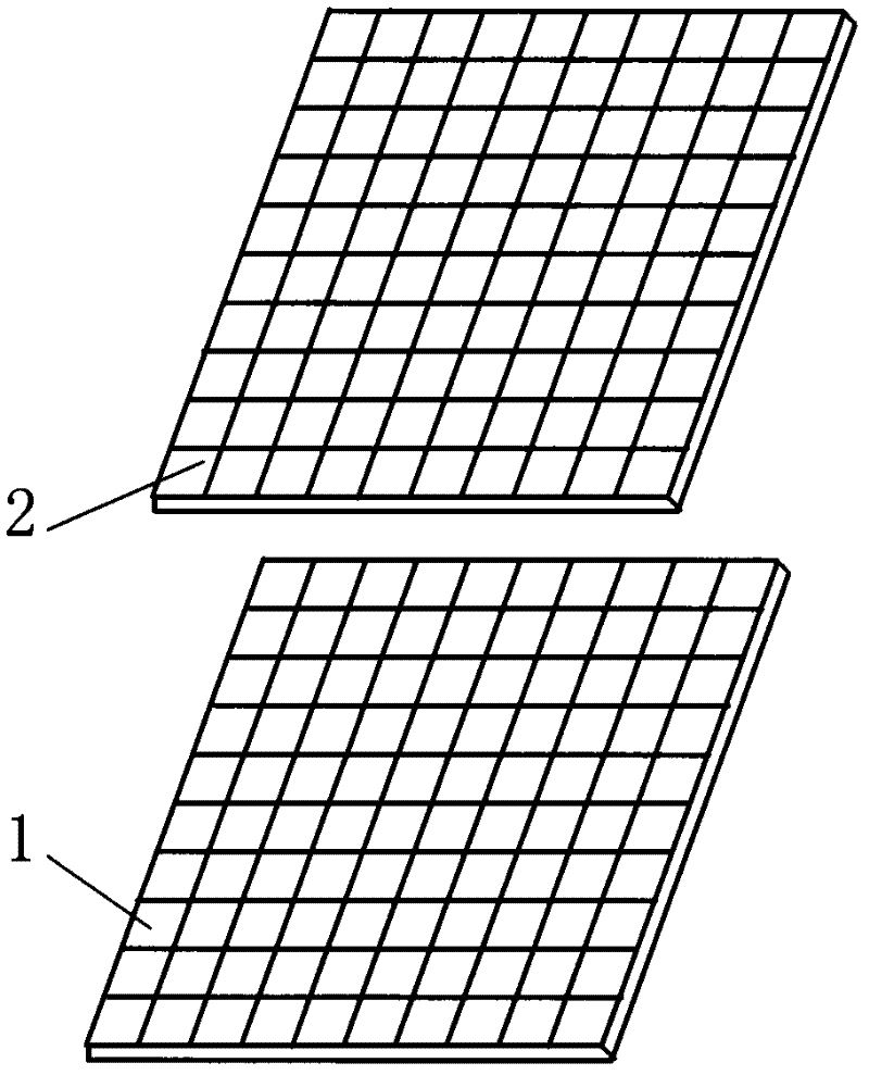
[0015] Firstly, the surface area of ​​the quasi-single crystal silicon wafer is divided into n×n grids, so that the area of ​​each grid occupies 1 / (n×n) of the area of ​​the entire quasi-single crystal silicon wafer 1 . Specifically, taking n=10 as an example, each grid represents 1 / 100 of the surface area of ​​a quasi-single crystal silicon wafer, that is, figure 1 shown.

[0016] Next, for the convenience of subsequent detection, the n×n array is fabricated on a transparent substrate through grid lines to form a two-dimensional grid scale 2 . Specifically, the manufacturing method of the two-dimensional grid ruler 2 adopted in the present invention is to use a photoplotter to draw at the central position of the film negative in a dark room. Afterwards, the film negatives that have undergone the light painting process are developed and fixed....


PUM

PropertyMeasurementUnit
Thicknessaaaaaaaaaa
Thicknessaaaaaaaaaa

Abstract

The invention relates to an appearance detection method of a quasi-monocrystalline silicon wafer, comprising the following steps of: firstly dividing the surface area of the quasi-monocrystalline silicon wafer into a grid of n*n arrays so as to make each grid area to account for 1(n*n) of the quasi-monocrystalline silicon wafer area; making a transparent substrate on the arrays through mesh lines to form a two-dimension grid gage; superposing the two-dimension grid gage with the edge of the silicon wafer; observing the surface of the silicon wafer through the transparent substrate of the two-dimension grid gage, finding the location distribution of monocrystalline crystal grains and polycrystalline crystal grains on the silicon wafer, and calculating; finally, multiplying the grid number of the monocrystalline crystal grains by 1 / (n*n) to calculate the area proportion of the monocrystalline crystal grains in the whole silicon wafer, and multiplying the grid number of the polycrystalline crystal grains by 1 / (n*n) to calculate the area proportion of the polycrystalline crystal grains in the whole quasi-monocrystalline silicon wafer. By the adoption of the method provided by the invention, the quality of the quasi-monocrystalline silicon wafer can be rapidly evaluated, and accuracy of the detection can be raised.

Description

technical field [0001] The invention relates to a detection method, in particular to an appearance detection method of a quasi-single crystal silicon wafer. Background technique [0002] At present, a method of producing quasi-monocrystalline silicon wafers by polycrystalline ingots has appeared in the market. This method combines the advantages of single crystal and polycrystalline to improve the competitiveness of products. The quasi-monocrystalline silicon wafers produced by the above method In addition to containing large-area monocrystalline grains, it is often unavoidable to have partially randomly grown polycrystalline grains. However, the ratio of the area of ​​single and polycrystalline grains to the area of ​​the entire silicon wafer is an important technical parameter of quasi-single crystal silicon wafers, which is used to evaluate the quality of quasi-single crystal silicon wafers. Currently there are no cheap and convenient quantitative methods and tools to me...

Claims


Application Information

Patent Timeline
IPC IPC(8): G01N21/95G01B11/28
Inventor 钱峰魏青竹孙利国任军林陆俊宇汪燕玲
Owner SUZHOU TALESUN SOLAR TECH CO LTD
Why Eureka
Try Eureka