
Carbon silicon-germanium silicon heterojunction 1T-DRAM (Single Transistor Dynamic Random Access Memory) structure on insulator and forming method thereof

A 1T-DRAM, insulator technology, applied in the manufacturing of transistors, semiconductor devices, semiconductor/solid-state devices, etc., can solve the problems of small signal current, limited increase in hole barrier, little increase in signal current and retention time, etc. The effect of operating voltage, increasing output current balance, and increasing signal margin

Active Publication Date: 2012-05-09
SHANGHAI HUALI MICROELECTRONICS CORP
View PDF5 Cites 2 Cited by
  • Summary
  • Abstract
  • Description
  • Claims
  • Application Information

AI Technical Summary

Problems solved by technology

However, the main problem of 1T-DRAM based on SOI structure is that the body potential is limited by the hole barrier between the acceptor region and the source and drain. Due to the limited band gap of conventional silicon semiconductors, the change of body potential is limited, and the change of threshold voltage is relatively small. Small (generally only about 0.3V), which makes the readout signal current smaller
However, the improvement of the hole barrier is limited, and the signal current and retention time are not greatly improved.

Method used


Image

  • Carbon silicon-germanium silicon heterojunction 1T-DRAM (Single Transistor Dynamic Random Access Memory) structure on insulator and forming method thereof
  • Carbon silicon-germanium silicon heterojunction 1T-DRAM (Single Transistor Dynamic Random Access Memory) structure on insulator and forming method thereof
  • Carbon silicon-germanium silicon heterojunction 1T-DRAM (Single Transistor Dynamic Random Access Memory) structure on insulator and forming method thereof

Examples


Embodiment Construction

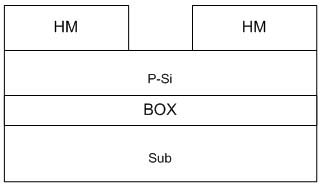
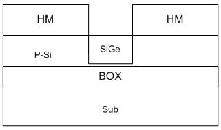
[0041] The present invention provides a carbon silicon-germanium silicon heterojunction 1T-DRAM structure, comprising: a semiconductor substrate, a buried oxide layer, the buried oxide layer covers the semiconductor substrate; a P-type silicon layer, the The P-type silicon layer is covered on the buried oxide layer, and the P-type silicon layer is provided with NMOS devices separated by STI, wherein the channel in the NMOS device is P-type SiGe.

[0042] The present invention will be further described below through the examples, so that the content of the present invention can be better understood, but the following examples do not limit the protection scope of the present invention.

[0043] The silicon-on-insulator silicon-germanium heterojunction 1T-DRAM structure provided by the present invention is formed by the following method.

[0044]A hard mask layer is deposited on the formed SOI wafer, and the hard mask layer is generally silicon nitride material. Carrying out pho...


PUM


Abstract

The invention provides a carbon silicon-germanium silicon heterojunction 1T-DRAM (Single Transistor Dynamic Random Access Memory) structure on an insulator, which comprises a semiconductor base plate, a buried oxide layer and a P-type silicon layer. The buried oxide layer covers the semiconductor base plate, the P-type silicon layer covers the buried oxide layer, and NMOS (N-channel Metal Oxide Semiconductor) devices separated by STI (Shallow Trench Isolation) are arranged on the P-type silicon layer, wherein channels of the NMOS devices are made of P-type germanium silicon. Compared with the prior art, the forming method disclosed by the invention can be applied to formation of the 1T-DRAM unit based on P-SiGe region+N+-SiCS / D, thus the working voltage can be effectively reduced; and simultaneously, output current balance between 0-reading and 1-reading is also increased, i.e. signal margin can be increased.

Description

technical field [0001] The invention relates to the technical field of semiconductors, in particular to a silicon-carbon-germanium-silicon-on-insulator heterojunction 1T-DRAM structure and a method for forming the structure. Background technique [0002] With the continuous shrinking of the feature size of semiconductor integrated circuit devices, in order to obtain sufficient storage capacitance (generally 30fF / cell) for traditional 1T / 1C embedded DRAM units, the capacitor preparation process (stack capacitor or deep trench capacitor) will It is becoming more and more complex, and the process compatibility with logic devices is getting worse and worse. Therefore, Capacitorless DRAM with good compatibility with logic devices will have a good development prospect in the field of high-performance embedded DRAM in VLSI. Among them, 1T-DRAM (One Transistor Dynamic Random Access Memory) has only 4F due to its unit size 2 It has become a research hotspot of non-capacitive DRAM a...

Claims


Application Information

Patent Timeline
Patent Type & Authority Applications(China)
IPC IPC(8): H01L29/10H01L29/08H01L27/108H01L21/8242H10B12/00
Inventor 黄晓橹陈玉文
Owner SHANGHAI HUALI MICROELECTRONICS CORP
Learn More